


TMS320C25, TMS320E25
SPRS010B — MAY 1987 — REVISED NOVEMBER 1990
POST OFFICE BOX 1443 • HOUSTON, TEXAS 77001
29
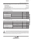
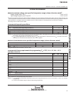
timing requirements over recommended operating conditions (see Note 3)
MIN NOM MAX UNIT
t
c(CI)
CLKIN cycle time 24.4 150 ns
t
f(CI)
CLKIN fall time 5
†
ns
t
r(CI)
CLKIN rise time 5
†
ns
t
w(CIL)
CLKIN low pulse duration, t
c(CI)
= 50 ns (see Note 4) 20 ns
t
w(CIH)
CLKIN high pulse duration, t
c(CI)
= 50 ns (see Note 4) 20 ns
t
su(S)
SYNC setup time before CLKIN low 5 Q – 5 ns
t
h(S)
SYNC hold time from CLKIN low 8 ns
†
Value derived from characterization data and not tested.
NOTES: 3. Q = 1/4t
c(C)
.
4. CLKIN duty cycle [t
r(CI)
+ t
w(CIH)
]/t
c(CI)
must be within 40-60%.
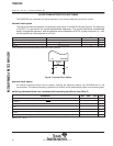
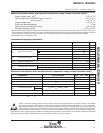
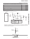
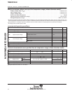
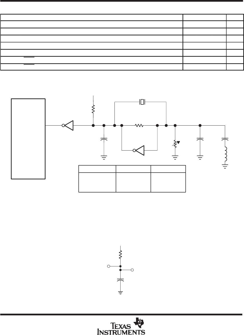
+5 V
f
crystal
4.7 kΩ
10 kΩ
74HC04
F11
CLKIN
47 pF
74AS04
10 kΩ
C = 20 pF 0.1 µF
L
TMS320C25
TMS320C25
TMS320C25-50
TMS320E25
40.96
51.20
40.96
1.8
1.0
1.8
f
crystal,
(MHz) L, (µH)
Figure 3. External Clock Option
Shown above is a crystal oscillator circuit suitable for providing the input clock signal to the TMS320C25,
TMS320E25, and TMS320C25-50. Please refer to
Hardware Interfacing to the TMS320C25
(document number
SPRA014A) for details on circuit operation.
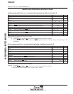
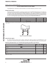
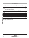
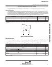
C
L
= 100 pF
2.15 V
R
L
= 825 Ω
Test
Point
From Output
Under Test
Figure 4. Test Load Circuit
ADVANCE INFORMATION