


TMS320E25
SPRS010B — MAY 1987 — REVISED NOVEMBER 1990
POST OFFICE BOX 1443 • HOUSTON, TEXAS 77001
60
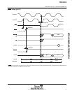
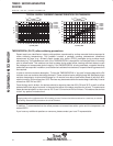
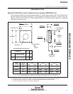
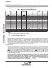
Table 5 shows the programming levels required for programming, verifying and reading the EPROM cell. The
paragraphs following the table describe the function of each programming level.
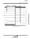
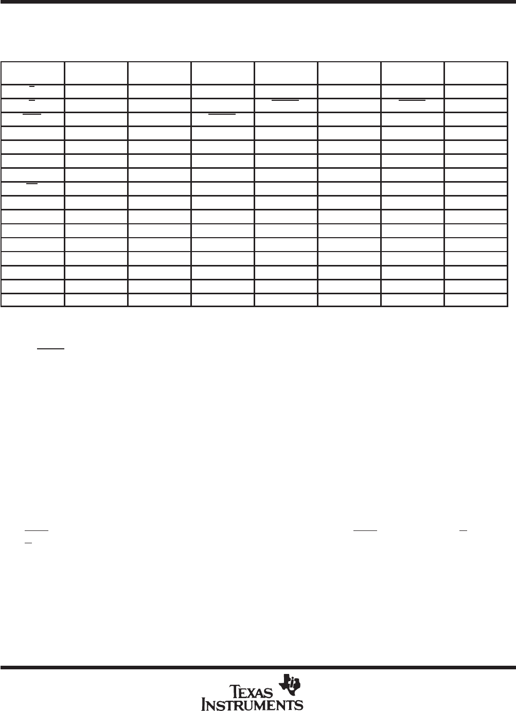
Table 5. TMS320E25 Programming Mode Levels
SIGNAL
NAME
†
TMS320E25
PIN
TMS27C64
PIN
PROGRAM
PROGRAM
VERIFY
PROGRAM
INHIBIT
READ
OUTPUT
DISABLE
E 22 20 V
IL
V
IL
V
IH
V
IL
V
IL
G 42 22 V
IH
PULSE X PULSE V
IH
PGM 41 27 PULSE V
IH
X V
IH
V
IH
V
PP
25 1 V
PP
V
PP
V
PP
V
CC
V
CC
V
CC
61,35 28 V
CC+1
V
CC+1
V
CC+1
V
CC
V
CC
V
SS
27,44,10 14 V
SS
V
SS
V
SS
V
SS
V
SS
CLKIN 52 14 V
SS
V
SS
V
SS
V
SS
V
SS
RS 65 14 V
SS
V
SS
V
SS
V
SS
V
SS
EPT 24 26 V
SS
V
SS
V
SS
V
SS
V
SS
Q1-Q8 18-11 11-13,15-19 D
IN
Q
OUT
HI-Z Q
OUT
HI-Z
A12-A10 40-38 2,23,21, ADDR ADDR X ADDR X
A9-A7 37,36,34 24,25,3 ADDR ADDR X ADDR X
A6 33 4 ADDR ADDR X ADDR X
A5 32 5 ADDR ADDR X ADDR X
A4 31 3 ADDR ADDR X ADDR X
A3-A0 30-28,26 7-10 ADDR ADDR X ADDR X
†
In accordance with TMS27C64.
LEGEND;
V
IH
= TTL high level; V
IL
= TTL low level; ADDR = byte address bit
V
PP
= 12.5 V ± 0.5 V; V
CC
= 5 ± 0.25 V; X = don’t care
PULSE
= low-going TTL level pulse; D
IN
= byte to be programmed at ADDR
Q
OUT
= byte stored at ADDR; RBIT = ROM protect bit.
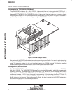
erasure
Before programming, the device is erased by exposing the chip through the transparent lid to high-intensity
ultraviolet light (wavelength 2537 Å). The recommended minimum exposure dose (UV-intensity ×
exposure-time) is 15 W•s/cm
2
. A typical 12 mW/cm
2
, filterless UV lamp will erase the device in 21 minutes. The
lamp should be located approximately 2.5 cm above the chip during erasure. After erasure, all bits are in the
high state. Note that normal ambient light contains the correct wavelength for erasure. Therefore, when using
the TMS320E25, the window should be covered with an opaque label.
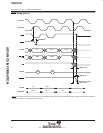
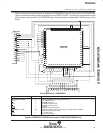
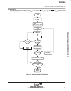
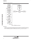
fast programming
After erasure (all memory bits in the cell are logic one), logic zeroes are programmed into the desired locations.
The fast programming algorithm, shown in Figure 10, is normally used to program the entire EPROM contents,
although individual locations may be programmed separately. A programmed logic zero can be erased only by
ultraviolet light. Data is presented in parallel (eight bits) on pins Q8-Q1. Once addresses and data are stable,
PGM
is pulsed. The programming mode is achieved when V
PP
= 12.5 V, PGM = V
IL
, V
CC
= 6 V, G = V
IH
, and
E = V
IL
More than one TMS320E25 can be programmed when the devices are connected in parallel. Locations
can be programmed in any order.
Programming uses two types of programming pulses: prime and final. The length of the prime pulse is 1 ms.
After each prime pulse, the byte being programmed is verified. If correct data is read, the final programming
pulse is applied; if correct data is not read, an additional 1-ms prime pulse is applied up to a maximum of 15
times. The final programming pulse is 4 ms times the number of prime programming pulses applied. This
sequence of programming and verification is performed at V
CC
= 6 V, and V
PP
= 12.5 V. When the full fast
programming routine is complete, all bits are verified with V
CC
= V
PP
= 5 V.
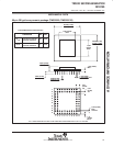
ADVANCE INFORMATION