


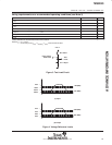

V
IL
T
A
Low-level
input
voltage
Operating
free-air
temperature
I
CC
Low-level input voltage T
A
= 0°C, V
CC
= MAX, f
x
= MAX
mA
TMS320C25, TMS320E25
SPRS010B — MAY 1987 — REVISED NOVEMBER 1990
POST OFFICE BOX 1443 • HOUSTON, TEXAS 77001
27
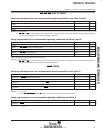
absolute maximum ratings over specified temperature range (unless otherwise noted)
†
Supply voltage range, V
CC
‡
– 0.3 V to 7 V. . . . . . . . . . . . . . . . . . . . . . . . . . . . . . . . . . . . . . . . . . . . . . . . . . . . . . . .
Input voltage range: TMS320E25 pins 24 and 25 – 0.3 V to 15 V. . . . . . . . . . . . . . . . . . . . . . . . . . . . . . . . . . . . .
All other inputs – 0.3 V to 7 V. . . . . . . . . . . . . . . . . . . . . . . . . . . . . . . . . . . . . . . . . . . . . . . . .
Output voltage range – 0.3 V to 7 V. . . . . . . . . . . . . . . . . . . . . . . . . . . . . . . . . . . . . . . . . . . . . . . . . . . . . . . . . . . . . .
Continuous power dissipation 1.5 W. . . . . . . . . . . . . . . . . . . . . . . . . . . . . . . . . . . . . . . . . . . . . . . . . . . . . . . . . . . . .
Operating free-air temperature range 0°C to 70°C. . . . . . . . . . . . . . . . . . . . . . . . . . . . . . . . . . . . . . . . . . . . . . . . . .
Storage temperature range – 55°C to 150°C. . . . . . . . . . . . . . . . . . . . . . . . . . . . . . . . . . . . . . . . . . . . . . . . . . . . . . .
†
Stresses beyond those listed under “Absolute Maximum Ratings” may cause permanent damage to the device. This is a stress rating only, and
functional operation of the device at these or any other conditions beyond those indicated in the “Recommended Operating Conditions” section of
this specification is not implied. Exposure to absolute-maximum-rated conditions for extended periods may affect device reliability.
‡
All voltage values are with respect to V
SS
.
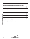
recommended operating conditions
MIN NOM MAX UNIT
V
CC
Supply voltage 4.75 5 5.25 V
V
SS
Supply voltage 0 V
All inputs except CLKIN/CLKX/CLKR/INT (0-2) 2.35 V
CC
+ 0.3 V
V
IH
High-level input voltage INT (0-2) 2.5 V
CC
+ 0.3 V
CLKIN/CLKX/CLKR 3.5 V
CC
+ 0.3 V
All inputs except MP/MC – 0.3 0.8 V
MP/MC – 0.3 0.8 V
I
OH
High-level output current 300 µA
I
OL
Low-level output current 2 mA
TMS320C25, TMS320E25 0 70 °C
TMS320C25GBA – 40 85 °C
electrical characteristics over specified free-air temperature range (unless otherwise noted)
PARAMETER TEST CONDITIONS MIN TYP
§
MAX UNIT
V
OH
High-level output voltage V
CC
= MIN, I
OH
= MAX 2.4 3 V
V
OL
Low-level output voltage V
CC
= MIN, I
OL
= MAX 0.3 0.6 V
I
Z
Three-state current V
CC
= MAX –20 20 µA
I
I
Input current V
I
= V
SS
to V
CC
–10 10 µA
Normal 110 185
Idle/HOLD 50 100
C
I
Input capacitance 15 pF
C
O
Output capacitance 15 pF
§
All typical values are at V
CC
= 5 V, T
A
= 25°.
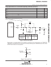
Caution. This device contains circuits to protect its inputs and outputs against damage due to high static voltages or electrostatic
fields. These circuits have been qualified to protect this device against electrostatic discharges (ESD) of up to 2 kV according to
MIL-STD-883C, Method 3015; however, it is advised that precautions to be taken to avoid application of any voltage higher than
maximum rated voltages to these high-impedance circuits. During storage or handling, the device leads should be shorted together
or the device should be placed in conductive foam. In a circuit, unused inputs should always be connected to an appropriate logic voltage level,
preferably either V
CC
or ground. Specific guidelines for handling devices of this type are contained in the publication “Guidelines for Handling
Electrostatic-Discharge Sensitive (ESDS) Devices and Assemblies” available from Texas Instruments
ADVANCE INFORMATION