Theory of Operation
Detailed Circuit Description
4
4-27
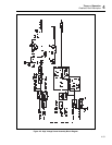
Transconductance and Cascode Stage 4-45.
The output voltage of the input amplifier U602, LVAMP, is transformed into a current
by Q602. The nominal current is about 8.5 mA. This implies that the nominal output
voltage of the input amplifier is about 6V; 15V - (.0085 * 1000) - .6 = 5.9V.
The current is passed through a cascode FET Q661, which can stand off the voltage
required, about 400V. A zener diode similar to VR656 protects most of the power
MOSFETs from damage to their gate oxide layer by excessive gate voltage
(approximately ±20V). A gate resistor similar to R675 suppresses high frequency
oscillations.
Midstage 4-46.
The current from Q661 generates a voltage of about 8.5V across R698. The ac voltage
gain from TP602, the LVAMP output, to R698 is unity. Transistor Q666 mirrors the
current into the midstage with an ac gain of 5. The dc midstage current is about 28 mA.
The midstage current passes through two cascode FETs, Q662 and Q665, to bias resistor
R674. Transistor Q660, VR658, and R678 form a 21 mA current source that, along with
R674 establishes the midstage bias current at about 28 mA. FET Q653 is a current
source from the +400V supply controlled by the auto-bias circuitry. The bias for Q654
and Q662 comes from the high voltage heat sink assemblies and is maintained about
halfway between the output voltage and the +400V supply or -400V supply, respectively.
The bias for Q665 comes from zener VR665, FET Q667, and its associated parts, which
form a 3 mA current source to bias the zener.
Zener VR661 provides some additional protection for Q665 and Q666. Capacitor C660
and R612 provide the dominant pole to stabilize the midstage amplifier. Gain-bandwidth
is set to about 7 MHz.
Midstage -400V Filter 4-47.
FET Q670 is a filter to reduce the 120 Hz and output signal ripple on the -400V supply.
Zener VR663, acting as a normal diode, clamps the gate of Q670 at the positive peak of
the ripple on the -400V supply. As soon as the -400V supply moves away from the
positive peak, the gate voltage is heavily filtered by R695 and C663. The zener action of
VR663 and VR664 prevents Q670 from being damaged by excessive gate voltage as the
-400V supply is turned on.
High Voltage Heat Sink Assemblies 4-48.
The output power MOSFET devices are mounted in pairs on the four high voltage heat
sink assemblies. Each pair is driven with the same gate voltage. To ensure they equally
divide the current, the MOSFETS are matched for gate-source voltage at 0.5A and have
3.9Ω source resistors. The push-pull output stage consists of Q655 and Q656 on the N-
channel heat sink assembly #2 and Q663 and Q664 on the P-channel heat sink assembly
#2. Their gates are driven with the voltage on R674. Resistors R670 through R673 sense
the output current, while Q658 and Q659 limit the current to about 2.4A. Diodes CR652
and CR654 help to reduce the amount of stored charge in the power MOSFETs that must
be driven when they are turned on and off.
The power MOSFETs on the #1 heat sink assemblies are driven cascode to share the
voltage drop between the output (MVOUT) and their respective 400V supply. This also
balances their power dissipation with the #2 heat sink assemblies. Their gates are driven
from the voltage divider R654 and R661 or R684 and R692. Capacitors C654 and C661


