5725A
Instruction Manual
4-32
• Serial Interface/Guard Crossing Section
The serial interface/guard crossing section consists of an RS-232 interface integrated
circuit that provides the hardware for 5700A/5725A communication within the
5725A. Two optoisolators provide the serial guard crossing to the Digital assembly
(A5), and two more provide integrity checks for the interface. A relay remotely
powered by the 5700A provides a software independent path to guarantee 5725A
shutdown if the 5700A/5725A cable is disconnected.
• Analog Input Switching Section
The analog input switching section consists of a bank of relays that route ac and dc
voltages and dc currents from the 5700A to various functional blocks inside the
5725A. Assemblies that receive inputs from the Analog Input Switching Section are
the High Voltage Amplifier assembly (A3); the Current Amplifier assembly (A2);
and the sense amplifier section of the High Voltage Sense assembly.
• Control Section
The control section is implemented with a bank of four latches connected to the
microprocessor data bus. A pair of latches with their integral drivers control relays, a
pair of latches control the 16-channel multiplexer and the bipolar output dac in the
analog monitor section.
• AC Line Voltage Switching Section
The ac line voltage switching section is independent of the other five sections of the
High Voltage Sense assembly. The ac line voltage section contains three switches
(labeled S2, S3, and S4 on the rear panel) that configure the input to the transformer
to accept one of eight nominal line voltage levels. Also included in this section are a
simple unregulated power supply and a time delayed relay driver circuit. These
circuits control a shunt switch around a pair of surge current-limiting NTC
thermistors.
Caution
To avoid meter damage, do not measure the ac line voltage
section unregulated supply with a meter tied to earth ground.
Sense Amplifier Section 4-55.
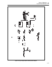
Op amp U102, transistors Q100 through Q103, and their associated parts comprise the
forward gain elements of a precision ac amplifier. Since this monolithic device does not
accept supply voltages large enough to accommodate output swings of ±15.6V, a quartet
of discrete transistors is configured as an output stage with voltage gain. This provides
the necessary output swing of 11V rms as well as limits the additional forward gain of
the overall amplifier to simplify frequency compensation.
Inputs to the output voltage stage are derived from deviations of the supply current of
U102 from its quiescent value. This topology depends on the increase in current from a
particular power supply as the output of the monolithic op amp moves toward the value
of that power supply. This increasing current develops a drop across R108 for positive
output voltages or a drop across R116 for negative output voltages. These drops are
amplified by Q100 and Q103. Transistors Q101 and Q102 buffer the output signal to
present a low source impedance to the load.
Overall gain at low frequencies is controlled by Z100, a resistor network designed for
good ac frequency response, low power coefficient, and low thermal settling time. This
network provides a feedback ratio of 0.99, or a closed-loop gain of 0.01. As a result, the
entire sense amplifier is running in a virtual unity gain configuration. Zeners VR103 and


