Theory of Operation
Detailed Circuit Description
4
4-33
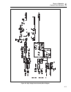
VR105 reduce apparent supply voltage seen by U102. Transistors Q105 and Q106 along
with R131/C117 and R132/C118 filter the supply to reduce common mode errors at high
frequency.
Capacitor C108 provides ac tuning for the sense amplifier. This capacitor balances most
of the parasitic capacitance picked up across the input resistor portion of Z100. Capacitor
C109, in parallel, provides fine adjustment of response if needed.
Components L105 and R130 isolate capacitive loads from the output of the sense
amplifier to aid in achieving stability. Transistor Q104 is necessary to route the output of
the sense amplifier to the 5700A during calibration. The signal routes to the B-RCL line
(the high-quality dc line to the 5700A calibration circuitry) through the analog monitor
section’s 16-channel multiplexer. This device cannot handle the output swing of the
sense amplifier (±15.6V) without risking inadvertent functional failure because of its
±15V supply limits. The result is to isolate the multiplexer from the sense amplifier
output during normal operation with the JFET switch Q104, which is then also turned on
during calibration. This is possible because the output of the sense amplifier is nominally
±3.2V during calibration.
During ac voltage operation, the input of the sense amplifier is either locally driven via
K104, or remotely driven via K105 and K109, by the High Voltage Amplifier assembly
(A3).
Op amp U103 forms a simple low offset voltage, low input current buffer to isolate the
B-SENSE LO line from the rest of the 5725A circuitry. B-SENSE LO is the reference
sense signal from the load provided through the 5700A and 5700A/5725A cable.
Buffering B-SENSE LO ensures that the current flowing between the load and the
5700A Switch Matrix assembly along this reference sense line is minimized, and as a
result, the series voltage drop is minimized.
The buffered B-SENSE LO line is distributed throughout the 5725A as MCOM,
MCOMI, MCOMV, and MCOMC. These lines are all at the same potential, but they
have different names corresponding to different paths taken to control the flow of ground
currents. These names correspond to destinations as shown in Table 4-3.
Table 4-3. High-Quality Reference Name Destination
REFERENCE NAME DESTINATION (ASSEMBLY)
MCOM High Voltage Sense (A6)
MCOMI Current (A2)
MCOMV Reference for high voltage input to calibration circuit, High Voltage Sense (A6)
MCOMC Calibration circuit section of the High Voltage Sense (A6)
The ac calibration circuit is also in the sense amplifier section. This circuit provides an
extremely flat ac response for 5725A calibration of the sense amplifier. This flat ac
response is made possible by the use of U101, the Fluke rms sensor, and a low-
impedance ranging resistor, R103. The value of this resistor is 50 times less than the
input resistor within Z100; as a result, the effect of parasitic capacitances is reduced by
2500. A protection circuit made up of CR101, CR102, VR101, and VR102 clamp input
voltages.
Op amp U100 is a forward gain block, configured as an integrator with U101. A
feedback circuit results, whose output at TP106 is a dc voltage proportional to the rms
value of the signal applied to R103 and the input sensing resistor of U101. Resistor R112
provides a simple means of protecting the output half of U101, while CR100 prevents


