OIGIT
ORIVER
SEGM€NT
DRIVER
MU
!TI
PLE
XER
PRESETAEL€
5-DIGIT
OECIMAL COUNTER
22-8lI r
16
ROM
GND
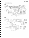
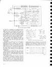
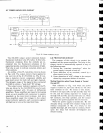
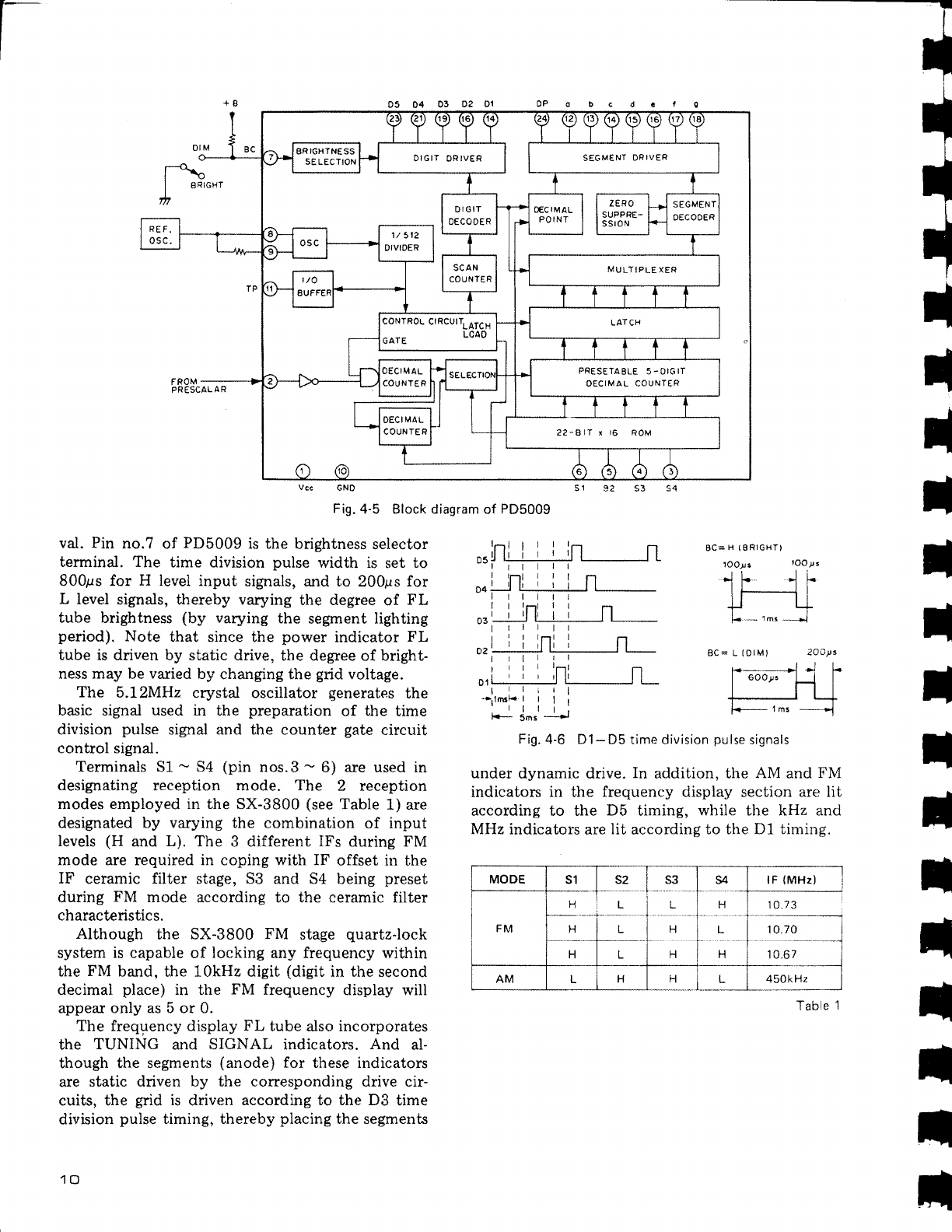
Fig.4-5
Block diagram
of
PD5009
I
I
I
I
I
I
I
t
I
r|
il
i
t
t
t
val. Pin
no.? of
PD5009
is the
brightness
selector
terminal. The
time division
pulse
width is
set
to
8009s
for
H level
input
signals, and to
200ps
for
L
level
signals, thereby varying
the degree
of
FL
tube brightness
(by
varying
the
segment lighting
period).
Note
that
since the
pov.er
indicator
FL
tube
is driven by static drive,
the degree
of
bright-
ness
may
be
varied
by
changing the
grid
voltage.
The
5.12MHz crystal
oscillator
generates
the
basic signai
used
in the
preparation
of
the
time
division
pulse
signal and
the
counter
gate
circuit
control signal.
Terminals S1
-
S4
(pin
nos.3
-
6) are used in
designating
reception mode.
The
2 reception
modes employed in the
SX-3800
(see
Table
1) are
designated by
varying
the combination
of input
levels
(H
and
L).
The
3 different
IFs
during
FM
mode are
required
in
coping
with IF
offset
in the
IF
ceramic filter stage, 53
and
54
being
preset
during
FM
mode according to the ceramic filter
characteristics.
Although
the SX-3800
FM
stage
quartz-lock
system
is
capable of
locking
any frequency within
the
FM
band, the L0kHz digit
(digit
in the second
decimal
place)
in
the
FM
frequency
display will
appear
only as 5 or 0.
The frequency display
FL
tube also incorporates
the TUNING and SIGNAL indicators.
And
al-
though the segments
(anode)
for these indicators
are
static driven by the corresponding drive
cir-
cuits, the
edd
is
driven
according to the D3
time
division
pulse
timing,
thereby
placing
the segments
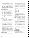
10
Inl
lttr-
o,w
ooM
*l-w
,,iw
-'l'*i*iill
t{--
tm3
+
8C= L
(DlM)
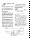
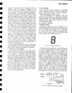
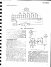
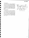
Fig.4-6
D1-D5
time division
pulse
signals
under
dynamic drive.
In
addition, the
AM
and
FIW
indicators
in
the
frequency display
section
are lit
according to the
Db
timing,
while the kHz and
MHz
indicators are
lit
accordine to
the D1 timine.
MODE
s1
S2
s3
I
H
L
H
lF
{MHz)
FM
H L L 1073
H
L H
H
10.70
H L
't
0.67
AM L
H H
L
450kHz
Table
1


