


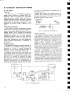
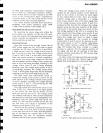

on the
other hand, the broadcasting
frequency
is
approached from
the
iow frequency
side
(or
when
tuning
away
to a lower frequency)
the
pin
no.4
voltage
will be lower,
resulting in
Q22
being tumed
on to light up
the
lower
frequency
(left
hand
side)
detuning
direction indicator. When
either
Q22
or
Q23
is
on, the
Q24
base voltage
will
be
high,
resulting
in
Q24
being
tumed on and
Q25
tumed
off,
which means
that the center tuning indicator
will not be lit up,
Once
the broadcasting
frequency
has
been
tuned
properly,
the voltages
on
pin
nos.2
& 4 will
be
equal. Consequently,
q22
and
Q23
will
both
be
turned
off, which
means
that
neither
of the detun-
ing
direction
indicators
will be
on in
this case. And
since
Q24
is
tumed
off because
of the
decreased
base voltage,
Q25
will
be turned
on, and
the
center
tuning
indicator
light up. Furthermore,
C77
is
charged
up via
R99,
resuiting
in
Q26
being
tumed
on, thereby
lighting
up
the
Quartz
Locked
indi-
cator
LED.
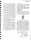
4.4 EOUALIZER
AMPLIFIER
?his
circuit
is
an
NFB
type equalizer
amplifier
with
newly
developed high
performance
IC
(HA1201?P).
This IC is
a low-noise
and
low distortion
type,
and
provide
an
openloop
gain
of 105d8.
The main
performance
specifications
for
this
circuit include
a
voltage
gain
of 35.5d8
(at
lkHz),
a
phono
dynamic
margin
or maximum
allowable
input
level
of 250mV
(1kHz,
0.}Abc/o THD),
S/N
ratio
of
82dB
(at
2.5mV
input,
IHF-A),
and equalization
within
t0.2dB
(20H2
*
20kHz).
4.5 TONE CONTROL AMPLIFIER
This
circuit is an
NFB
type tone control ampli-
fier with
newly developed high
performance
IC
iHA12017P).
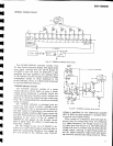
4.6
POWER
AMPLIFIER
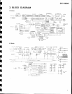
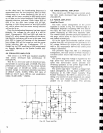
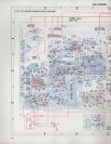
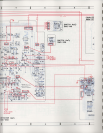
Amplifier
Circuit
The
basic
circuit arrangement of the
power
amplifier
is shown in
Fig.
4-9. The first
stage is a
differential
amplifier comprising
PNP
twin transis-
tor
(Q2),
the load
circuit of which is
a current
mirror
employing
an
NPN
twin transistor
(Q3).
The
current mirror
provides push-pull
operation in
this
stage, which
serues to cancel
even harmonics
and further
increase
gain.
Q1
in
the input
circuit absorbs
outflorv of base
current from
Q2,
and
prevents
the
generation
of a
DC voltage.
Because
Q1
follows
any temperature
drift
in
Q2,
temperature
drift of the center
point
voltage
is
prevented.
The
pre-driver
stage
(Q4,
Qb)
is a Darlington
arrangement,
the
load
circuit of which
employs
a
constant-current
source
(Q6)
resulting a high volt-
age
gain.
The
power
stage
bias voltage
is supplied
by the
high
speed bias
servocontrol circuit. The high
speed
bias
servocontrol circuit
provides
non-
switching
operation in
the
power
stage
(refer
to
"High
Speed Bias
Servocontrol Circuit").
The
power
stage
(Q13
-
Q16)
is
a 2-stage Dari-
ington
arrangement,
the last
stage
is
SEPP circuit
employing
an SL
RET
(Super
Linearit5' Ring
Emitter
Transistor).
The RET
is a kind
of
IC
con-
sisting
of a number of
smail
transistors
on a single
chip,
with
each transistor being connected ir"r
parallel
via
an emitter resistor. This
provides
t
t
t
H
H
H
t
I
t
n
i
+
I
i
;
+
I
+
I
td
Fig.
4-9
Power
amplifier