5 220A
Instruction Manual
3-6
3-8. Preamplifier
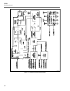
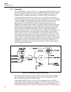
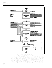
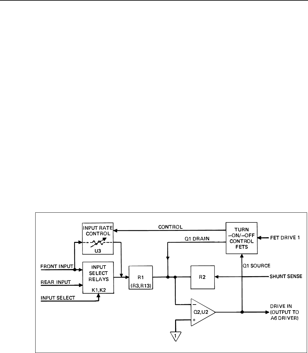
The A5 Preamplifier, as shown in Figure 3-4, is a high-gain amplifier designed to accept
a front/rear panel input signal and provide an amplified output to the A6 Driver stage of
the transconductance amplifier. It consists of a high-gain differential amplifier with
feedback resistors, front/rear input select relays, and turn-on/off control circuitry.
In operation, the input voltage source (front or rear), as selected by the A10 Logic, is
connected through reed relay K1 (front) or K2 (rear) and input resistors R1, R3, and R13
to the inverting input of a differential transistor pair, Q2. The non-inverting input of Q2 is
connected to COM 1 through parallel resistors R9 and R14. The resistance value
approximates the value of R1 and R2 in parallel and, thereby balances the source
impedance at the amplifier inputs. Balance is required to minimize apparent input offset
voltage that may result from input currents. Diode CR3 and diode-connected transistor
Q3 are voltage clamps that prevent amplifier saturation on high input transients. The
collectors of Q2A and Q2B drive the emitters of a pair of grounded base amplifiers
formed by transistor array, U1. This holds the collectors of Q2 at a low and equal level to
maintain low and equal collector-to-base leakage currents (ICER) at Q2. The actual
collector voltage of Q2 is set by the temperature corrected divider formed by R4, R19,
and the diode connected transistor U1C. Voltage variations at the collectors of U1A and
U1B constitute the output of the differential amplifier, and are used as the input to op-
amp, U2. Diodes CR4 and CR5 clamp the inputs to prevent U2 saturation when transient
voltages appear. An ac feedback network, R15 and C7, fix the frequency response of the
preamplifier to satisfy the overall transconductance amplifier loop. Amplifier zero is
established by the selected values of collector resistors R11 and R12, and the setting of
the zero-adjust potentiometer, R6.
ajs09f.wmf
Figure 3-4. A5 Preamplifier Functional Block Diagram
The turn-on/off control FET (Q1) operates as FET switch to control the overall gain of
the A5 Preamplifier in both the standby and operate modes. Q1 responds to the FET
Drive 1 signal initiated (as T2) on the A10 Logic.
In the standby mode FET Drive 1 is near zero volts causing Q1 to turn on. FET Q1
completes the feedback loop between the output of U2 and the inverting input of Q2. This
in effect reduces the gain of the A5 Preamplifier to zero. As a result the output of the
transconductance amplifier is forced to zero amperes. Photo resistor U3 is used to control


