5 220A
Instruction Manual
3-8
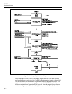
string is used as a voltage source to set the quiescent bias for the remaining stages of the
complementary A7 Driver and A7 Output. Variable resistor R13 is used to set the initial
bias voltage.
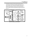
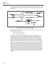
ajs10f.wmf
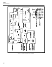
Figure 3-5. A6 Driver Functional Block Diagram
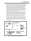
The characteristics of the VBE multipliers used in the bias section are stated in terms of
Q5 in the following formulas:
VBE = [R14/R14 + R15] VCE
VCE = VBE [R14 + R15/R14]
The output section of the A6 Driver consists of transistors Q8, Q9, Q10, Q12, and
associated components. Transistors Q8 and Q9 are arranged as complementary emitter
followers that are both biased and driven by the bias section. This is followed by a
common collector stage using Q10 and Q12. Overcurrent protection is provided in the
stage by the 10 ohms resistors, R30 and R31, in the collector circuits. The differential
output at the emitters of Q10 and Q12 is used as the drive input to the A7 output stage.
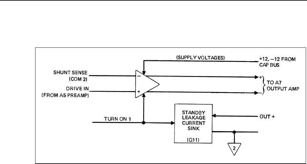
In the standby mode of operation it is necessary to reduce the 5220A output to a zero-
volt/zero-current condition. This is accomplished on the A6 Driver by two separate FET
circuits. FETs Q6 and Q7 comprise the voltage shut-down circuit, and FET Q11 is the
output current-sink. Both are enabled by a Turn-on 1 signal which is initiated (as T1) by
the A10 Logic when the 5220A is switched to standby. When Q6 and Q7 are enabled
(turned on) they remove the bias from the output stage of the A6 Driver, and thereby
disable the bias to the A7 Output stage. In this state the output is essentially floating and
is influenced only by leakage current that may be present in the output drivers. FET Q11
remedies the floating condition by effectively clamping the output to output common
(COM 2).


