Theory of Operation
Circuit Analysis
3
3-7
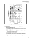
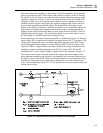
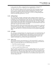
the rate at which the input voltage is applied to the A5 Preamplifier when the 5220A is
switched from standby to operate. This is necessary to prevent a step output which, if
applied to an inductive load, would result in an overvoltage transient, forcing the 5220A
back to standby. In standby both input select relays, K1 and K2, are open, capacitors, C3
and C12, are discharged, and the photo resistor U3 is a very high impedance with the
LED drive removed. Thus, the A5 Preamplifier is effectively isolated from the input
voltage.
In the operate mode FET Drive 1 is stepped to –15 V dc causing FET Q1 to turn off.
With Q1 off, the A5 Preamplifier returns to its high gain state with feedback established
by resistors R1 and R2. If front input is selected, the Relay 1 drive signal is low and
capacitor C12 begins charging. The increasing voltage across C12 increased the LED
output from U3 which, in turn, decreases the impedance of the photo resistor. Since the
resistor is in parallel with the input contacts of the still open front input relay K1, it acts
as a variable input attenuator. In other words, the front input voltage is applied to the
input of the A5 Preamplifier at a controlled rate and not as a step input. At the same time,
a low Relay 1 drive signal is inverted by U4 causing C3 to charge through R24. When the
charge reaches the threshold of the second inverter (U4) relay K1 is energized by a set of
four parallel connected inverters. The charge time for C3 and C12 are designed to ensure
that K1 closes after photo resister U3 changes to a low impedance. When K1 closes, it
places a short across the resistor in U3 and selects the front panel input voltage to drive
the A5 Preamplifier. If the rear panel input signal is selected, a variable attenuator is not
necessary because the signal from the remote 5100A rises at a controlled rate when
switched from standby to operate.
3-9. A6 Driver
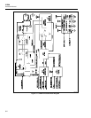
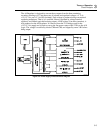
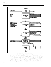
The A6 Diver, as shown in Figure 3-5, is a differential amplifier designed to accept its
input from the A5 Preamplifier and to provide a differential drive signal to the A7 Output
stage. The amplifier itself is of a discrete-component, complementary, push-pull design.
Its features include the following:
• Temperature compensated biasing for both itself and the A7 Output stage
• An amplifier-disable circuit for standby operation
• An output-leakage current sink for standby operation.
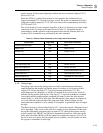
The input section of the driver amplifier consists of a differential transistor pair, Q2 and
Q3; a current regulator, Q4; and a common base driver, Q1, for the bias circuit.
Transistor Q3 of the input pair receives the drive input from the A5 Preamplifier. The
other input transistor, Q2, is driven by Shunt Sense 2, which provides negative feedback
from the output current shunt to reduce distortion in the A7 Output stage. Current
regulator Q4 regulates the emitter current of the differential pair, and provides isolation
from variations in the –12 V supply. Output from the differential pair is taken at the
collector of Q3 by way of a common-base driver, Q1.
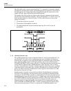
The bias section of the driver amplifier consists of resistors, R13 through R17, current
regulator, CR1, and transistors, Q5 and Q107 (Q107 is physically located on the output
amplifier's heat sink). Resistors R13 through R17 and current regulator CR1 form a series
string that is driven by the output driver Q1 of the input amplifier. Regulator CR1 is at
the end of the string and connected to –12 V dc. This ensures a constant current of
approximately 5.2 mA through the string. Transistors Q5 and Q107 are connected across
resistors R14, R15 and R16, R17 as VBE multipliers to ensure that the voltage drop
across the resistor string changes at a rate which will compensate for VBE temperature
changes in the A6 Driver and A7 Output stages. Transistor Q5 senses ambient
temperature changes while Q107 senses temperature changes due to power dissipation in
the A7 output. The temperature compensated voltage drop developed across the resistor


