5 220A
Instruction Manual
3-10
3-11. A8 Analog Control
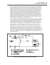
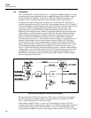
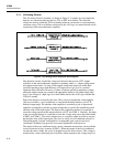
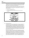
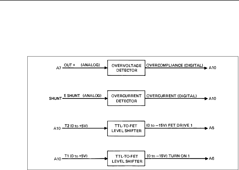
The A8 Analog Control Assembly, as shown in Figure 3-7, contains an overcompliance
detector, an overcurrent detector and two TTL-to-FET level shifters. The detection
circuits are used to switch the 5220A to standby when an overcurrent or overcompliance
condition occurs. The level shifters are driven by the A10 Logic to control the turn-on/off
sequencing of the transconductance amplifier.
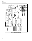
ajs12f.wmf
Figure 3-7. A8 Analog Control Simplified Block Diagram
The detection circuits are absolute value level detectors that provide a TTL output
indication of the transconductance amplifier’s operating status; i.e., output voltage status
and output current status. As long as both output voltage and current are within their
specified operating range, both detectors will output a low logic level as a normal-
operation status indication. However, if either or both the specified compliance voltage
and/or the output current are exceeded, the appropriate detector will output a high logic
level. Upon receipt of a high logic level from either detector the A10 Logic switches the
5220A to standby.
Each of the detectors is basically the same. They consist of an absolute value amplifier
(full-wave rectifier), a level conditioner, a zener diode threshold detector, and a TTL
buffered output stage. The absolute value amplifier is essentially a pair of operational
amplifiers configured to provide an output voltage that is equal to the amplified positive
absolute value of the input signal. The input to the compliance detector is connected to
sense the voltage present at the output terminals (+OUT and COM 1). Similarly, the input
to the overcurrent detector is connected to sense the voltage drop across the current shunt
(COM 2 and COM 1). The result, in both cases, is a negative output level that is equal to
the absolute value of the input signal. This level is sent to a level conditioner where it is
filtered/integrated, inverted, and amplified. An adjustable gain control in the level
conditioner’s feedback loop provides for accurate adjustment of the trip level.
The output of the level conditioner feeds a series connected zener/resistor circuit with the
resistor connected to logic common (COM 3). When the output of the level conditioner
exceeds the zener voltage, the excess is dropped across the zener resistor. This voltage is
monitored by a series-connected-pair of inverters which respond to the voltage drop as if


