


v
List of Tables
Table Title Page
1-1. Accessories ............................................................................................................ 1-2
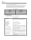
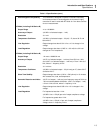
1-2. Specifications......................................................................................................... 1-2
2-1. Controls, Indicators, and Connectors..................................................................... 2-4
3-1. Effect of Reset Command on A10 Logic and A9 Front Panel............................... 3-13
4-1. Required Test Equipment ...................................................................................... 4-1
4-2. DC Accuracy Test.................................................................................................. 4-10
4-3. Frequency Response Test ...................................................................................... 4-11
4-4. Replacement Resistors for R11 and R12 ............................................................... 4-17
4-5. Replacement Resistors for R13.............................................................................. 4-18
4-6. Mainframe and Digital Section Troubleshooting Guide........................................ 4-21
4-7. Analog Section Troubleshooting Guide................................................................. 4-25
5-1. 5220A Final Assembly .......................................................................................... 5-4
5-2. A1 Motherboard PCB Assembly ........................................................................... 5-17
5-3. A2 Power Transformer Assembly ......................................................................... 5-18
5-4. A3 Capacitor Bus PCB Assembly ......................................................................... 5-19
5-5. A4 Regulator PCB Assembly ................................................................................ 5-21
5-6. A5 Preamplifier PCB Assembly............................................................................ 5-23
5-7. A6 Driver PCB Assembly...................................................................................... 5-26
5-8. A7 Output PCB Assembly..................................................................................... 5-28
5-9. A8 Analog Control PCB Assembly....................................................................... 5-31
5-10. A9 Front Panel PCB Assembly.............................................................................. 5-33
5-11. A10 Logic PCB Assembly..................................................................................... 5-34
5-12. A11 MIS Bus Interface PCB Assembly................................................................. 5-36
5-13. A12 Shunt Assembly ............................................................................................. 5-38
5-14. A13 Output Termination PCB Assembly .............................................................. 5-40
5-15. A14 Extender PCB Assembly................................................................................ 5-41