


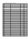
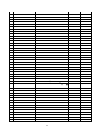
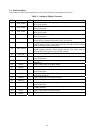
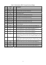

41
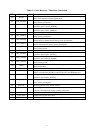
Table 3 : Clock Recovery / Time Base Conversion
PIN # Name I/O Description
125 DVDD
Digital power for Destination DDS (direct digital synthesizer). Must be bypassed
with a 0.1uF capacitor to digital ground plane.
127 DAC_DGNDA
Analog ground for Destination DDS DAC. Must be directly connected to the
analog system ground plane.
128 DAC_DVDDA
Analog power for Destination DDS DAC. Must be bypassed with a 0.1uF
capacitor to pin 127 (DAC_DGNDA).
129 PLL_DVDDA
Analog power for the Destination DDS PLL. Must be bypassed with a 0.1uF
capacitor to pin 131 (PLL_DGNDA).
130 Reserved
For testing purposes only. Do not connect.
131 PLL_DGNDA
Analog ground for the Destination DDS PLL. Must be directly connected to the
analog system ground plane.
132 SUB_DGNDA
Dedicated pin for the substrate guard ring that protects the Destination DDS.
Must be directly connected to the analog system ground plane.
133 SUB_SGNDA
Dedicated pin for the substrate guard ring that protects the Source DDS. Must be
directly connected to the analog system ground plane.
134 PLL_SGNDA
Analog ground for the Source DDS PLL. Must be directly connected to the
analog system ground.
135 Reserved
For testing purposes only. Do not connect.
136 PLL_SVDDA
Analog power for the Source DDS DAC. Must be bypassed with a 0.1uF
capacitor to pin 134 (PLL_SGNDA)
137 DAC_SVDDA
Analog power for the Source DDS DAC. Must be by passed with a 0.1uF
capacitor to pin 138 (DAC_SGNDA)
138 DAC_SGNDA
Analog power for the Source DDS DAC. Must be directly connected to the
analog system ground.
139 SVDD
Digital power for the Source DDS. Must be bypassed with a 0.1uF capacitor to
digital ground plane.
141 TCLK I Reference clock(TCLK) input from the 50 MHz crystal oscillator
142 XTAL O If using an external oscillator, leave this pin floating. If using an external crystal,
connect crystal between TCLK(141) and XTAL(142). See MFB5(pin 107).
143 PLL_RVDDA Analog power for the Reference DDS PLL. Must be bypassed with a 0.1uF
capacitor to pin 144(PLL_RGNDA)
144 PLL_RGNDA Analog ground for the Reference DDS PLL. Must be directly connected to the
analog system ground plane.
145 Reserved For testing purposes only. Do not connect.
146 SUB_RGNDA Dedicated pin for the substrate guard ring that protects the Reference DDS. Must
be directly connected to the analog system ground plane.
148 VSYNC I CRT Vsync input. TTL Schmitt trigger input.
149 SYN_VDD Digital power for CRT Sync input.
150 HSYNC/CSYNC I CRT Hsync or CRT composite sync input. TTL Schmitt trigger input.