


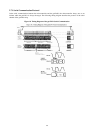

63
3. ELECTRICAL CHARACTERISTICS
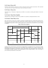
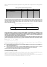
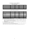
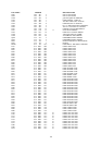
Table 20. Absolute Ratings
Parameter Min. Typ. Max. Note
PVDD 5.6 volts
CVDD 5.6 volts
Vin Vss-0.5 volt Vcc+0.5V
Operating temperature 0 degree C 70 degree C
Storage temperature -65 degree C 150 degree C
Maximum power consumption ~2W
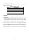
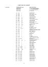
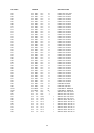
Table 21. DC Electrical Characteristic
Parameter Min. Typ. Max. Note
PVDD 3.15 volts 3.3 volts 3.47 volts
CVDD 3.15 volts 3.3 volts 3.47 volts
Vil (COMS inputs)
Vil (TTL inputs)
0.3*CVDD
0.8 volts
Vih (COMS inputs)
Vih (TTL inputs)
0.7 * CVDD
2.0 volts
1.1*CVDD
5.0+0.5 volts
(1)
Voh 2.4 volts CVDD
Vol 0.2 volts 0.4 volts
Input Current -10 uA 10 uA
PVDD operating supply current 0 mA 20 mA/pad @ 10pF (2)
CVDD operating supply current 0 mA 500 mA (3)
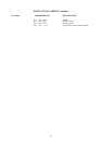
NOTE 1:5V-Tolerent TTL Input pads are as follows:
z CRT Interface: HSYNC (pin #150), VSYNC (#148)
z Host Interface: HFS (#98), HCLK (#103), HDATA (#99), RESETN (#100), MFB[11:0]: MFB11 (#123),
MFB10 (#124), MFB9 (#102), MFB8 (#104), MFB7 (#105), MFB6 (#106), MFB5 (#107), MFB4 (#109),
MFB3 (#110), MFB2 (#111), MFB1 (#112), MFB0 (#113)
z OSD Interface: OSD_DATA3 (#121), OSD_DATA2 (#120), OSD_DATA1 (#119), OSD_DATA0 (#118),
OSD_FSW (#122)
z Non-5V-Tolerant TTL Input Pad is: TCLK(#141)
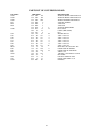
NOTE 2: When the panel interface is disabled, the supply current is 0 mA. The drive current of each pad can be
programmed in the range of 2 mA to 20 mA (@capacitive loading = 10 pF)
NOTE 3: When all circuits are powered down and TCLK is stopped, the CVDD supply current becomes 0 mA.