


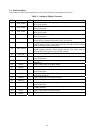
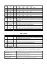
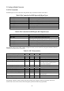
43
PIN # Name I/O
Description
2pxl/clk 2pxl/clk 1pxl/clk 1pxl/clk
8bit 6-bit 8-bit 6-bit TFT
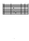
63 PD7 O EG3 EG1 G3 G1
64 PD6 O EG2 EG0 G2 G0
66 PD5 O ER7 EG5 R7 R5
67 PD4 O ER6 ER4 R6 R4
68 PD3 O ER5 ER3 R5 R3
69 PD2 O ER4 ER2 R4 R2
70 PD1 O ER3 ER1 R3 R1
71 PD0 O EG2 ER0 R2 R0
43 PdispE O This output provides a panel display enable signal that is active when flat panel
data is valid.
74 PHS O This output provides the panel line clock signal.
73 PVS O This output provides the frame start signal.
44 PCLKA O This output is used to drive the flat panel shift clock.
45 PCLKB O Same as PCLKA above.
The polarity and the phase of this signal are independently programmable.
75 Pbias O This output is used to turn on/off the panel bias power or controls backlight.
76 Ppwr O This output is used to control the power to a flat panel.
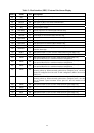
Table 5. Test Pins
PIN # Name I/O Description
3 PSCAN I
Enable automatic PCB assembly test. When this input is pulled high, the
automatic PCB assembly test mode is entered. An internal pull-down resistor
drives this input low for normal operation.
155 SCAN_IN1 I
Scan input 1 used for automatic PCB assembly tesing.
157 SCAN_IN2 I
Scan input 2 used for automatic PCB assembly tesing.
159 SCAN_OUT1 O
Scan output 1 used for automatic PCB assembly tesing.
160 SCAN_OUT2 O
Scan output 2 used for automatic PCB assembly tesing.
153 Reserved
154 Reserved
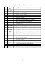
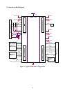
Table 6. VDD / VSS for Core Circuitry, Host Interface, and Panel/Memory Interface
PIN # Description
65, 40, 33, 12
PVDD4~PVDD1 for panel / memory interface. Connect to +3.3V.
Must be the same voltage as the CVDD’s
149, 108, 58, 21, 11
SRVDD2-1, CVDD4, CVDD2-1 for core circuitry. Connect to +3.3V.
Must be the same voltage as the PVDD’s.
158, 151, 140, 126, 114, 72, 61,
49, 41, 30, 18, 8, 1
Digital grounds for core circuiry and panel / memory interface.