


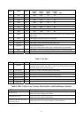
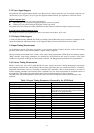

47
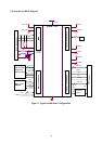
2. FUNCTIONAL DESCRIPTION
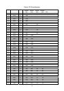
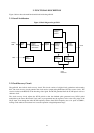
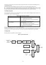
Figure 3 below shows the main functional blocks inside the gmZAN1
2.1 Overall Architecture
Figure 3. Block Diagram for gmZAN1
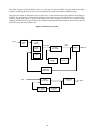
2.2 Clock Recovery Circuit
The gmZAN1 has a built-in clock recovery circuit. This circuit consists of a digital clock synthesizer and an analog
PLL. The clock recovery circuit generates the clock used to sample analog RGB data (SCLK or source clock). This
circuit is locked to the HSUNC of the incoming video signal. The RCLK generated from the TCLK input is used as a
reference clock.
The clock recovery circuit adjusts the SCLK period so that the feedback pulse generated every SCLK period
multiplied by the Source Horizontal Total value (as programmed into the registers) locks to the rising edge of the
Hsync input. Even though the initial SCLK frequency and the final SCLK frequency are as far apart as 60MHz ,
locking can be achieved in less than 1ms across the operation voltage/temperature range.
Triple
ADC
Source
Timing
Measurement
/ Generation
Scaling
Engine
Gamma
Control
(CLUT)
+
Dither
Panel
Timing
Control
On-Screen
Display
Control
Host
Interface
Clock
Recovery
Pixel
Clock
Generator
Analog
RGB
MCU
Panel
Clock
Reference