


NX-800/800H
19
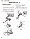
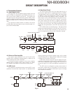
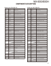
4. Transmitter System
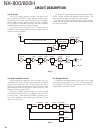
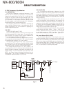
4-1. Audio Band Circuit
The signal from the microphone goes through the mute
switch (Q706), the Mic-Mute signal (MM) becomes Low,
then mute switch (Q706) is turned off. The signal from
microphone goes through Mic-AGC (Q704, Q705, D704,
D705), and goes through switch IC (IC708), and amplifi ed by
Mic-Amp IC706 (1/2), LPF IC706 (2/2) works as anti-aliasing
fi lter.
If an optional scrambler board is installed, the switch
(IC708) adjusts the signal path so that the audio signal is in-
put to the scrambler board.
4-2. Base Band Circuit
The audio signal output from the base band circuit is
converted to digital data of a sampling frequency of 48kHz.
This digital data is sent to the DSP (IC502), and voice signals
of 300Hz or lower and frequencies of 3kHz or higher are
cut off and an audio range 300Hz to 3kHz is extracted. The
audio signal is then pre-emphasized in FM mode and syn-
thesized with the signals, such as QT and DQT, as required,
and is then output from the IC510. In Digital mode, the au-
dio signal is converted to the 4-Level FSK base band signal
and output from the IC510. The DTMF and MSK base band
signals are also generated by the DSP and output by the
IC510.
LPF (IC702) works as smoothing fi lter. The DAC (IC712)
assigns the base band signal to the VCO and VCTCXO (X1).
At this time, the level output according to the transmit car-
rier is fi ne-adjusted according to each modulation method.
CIRCUIT DESCRIPTION
SW
Q707 IC708
MM
AMP
IC706
(1/2)
LPF
IC706
(1/2)
LPF
IC702
(1/2)
AMP IC712
IC709
(1/2)
IC510
IC502
DSP
LPF
IC702
(2/2)
AMP
IC1
AMP
VCTCXO
X1
VCO
IC5 (2/2)
AGC
D703,D704
Q705,Q706
SW
SCSW
Optional Scrambler Board
INT. MIC
Fig. 5
Fig. 6
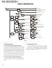
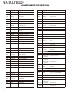
4-3. Drive and Final amplifi er
The transmit signal obtained from the TX VCO buffer
amplifi er Q9, is amplifi ed to approximately +17dBm by the
driver amplifi ers Q10, Q101 and Q102.
This amplified signal is passed to the power amplifier
module (power module) IC102, which consists of a MOS-
FET amplifi er and capable of transmission output power.
4-4. APC circuit
The Automatic transmission power control (APC) circuit
stabilizers the transmitter output power at a predetermined
level by detecting the power module output with a diodes
D108, D109 and D110. Diodes D108, D109 and D110 apply
a voltage to DC amplifi er IC103 (1/2).
IC103 (2/2) compares the APC control voltage (PC) gen-
erated by microprocessor IC510 and DC amplifi er IC101 (1/2,
2/2) with the detection output voltage from IC103 (1/2) to
control the Vgg Pin of IC102, and stabilizes transmission out-
put.
The APC circuit is confi gured to protect over-current of
the power module due to fluctuations of the load at the
antenna end and to stabilize transmission output at voltage
and temperature variations.
TX VCO
VCTCXO
19.2MHz
0dBm +17dBm
Drive AMP
Q10
Buff AMP
Q9
Drive AMP
Q101
Drive AMP
Q102
Final AMP
IC102
MOD
MB
DC
AMP
DC
AMP
PC
MP
SW ANT Filter
D103*,D104,
D106,D216
DET
D108
ANT
*D103: NX-800H only
Gate
bias
IC101 IC103
DET
D109
DET
D110