


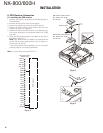
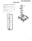
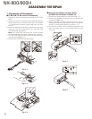
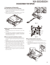

NX-800/800H
20
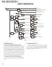
5. PLL Frequency Synthesizer
5-1. VCTCXO (X1)
VCTCXO (X1) generates a reference frequency of 19.2
MHz for the PLL frequency synthesizer. This reference
frequency is applied to pin 9 of the PLL IC (IC3) and con-
nected to IF circuit as a 2nd local signal through Tripler. The
VCTCXO oscillation frequency is determined by DC voltage
of VC terminal. The VC voltage is fi xed to 1.65V by R1 and
R2, and supplied to VC terminal through IC2. Modulation
signal is also fed to VC terminal through IC2.
The frequency adjustment is achieved by switching the
ratio of dividing frequency that is not adjusted by the DC
voltage impressed to VC. The resolution of adjusting fre-
quency is approximately 4Hz.
5-2. VCO
There is a RX VCO and a TX VCO.
The TX VCO (Q6) generates a transmit carrier and the RX
VCO (Q5) generates a 1st local signal. For the VCO oscil-
lation frequency, the transmit carrier is 450 to 520MHz and
the 1st local signal is 391.95 to 461.95MHz.
The VCO oscillation frequency is determined by one sys-
tem of operation switching terminal “T/R” and two systems
of voltage control terminals “C/V” and “V-assist”.
The operation switching terminal, “T/R”, is controlled by
the control line (/T_R) output from the MCU (IC510). When
the /T_R logic is low, the VCO outputs the transmit carrier
and when it is high, it outputs a 1st local receive signal.
The voltage control terminals, “CV” and “V-assist”, are
controlled by the PLL IC (IC3) and MCU (IC510) and the
output frequency changes continuously according to the
applied voltage. For the modulation input terminal, “VCO
MOD”, the output frequency changes according to the ap-
plied voltage. This is used to modulate the VCO output.
“VCO MOD” works only when “/T_R” is low.
5-3. PLL IC (IC3)
PLL IC compares the differences in phases of the VCO
oscillation frequency and the VCTCXO reference frequency,
returns the difference to the VCO CV terminal and realizes
the “Phase Locked Loop” for the return control. This allows
the VCO oscillation frequency to accurately match (lock) the
desired frequency.
When the frequency is controlled by the PLL, the fre-
quency convergence time increases as the frequency dif-
ference increases when the set frequency is changed. To
supplement this, the MCU is used before control by the PLL
IC to bring the VCO oscillation frequency close to the de-
sired frequency. As a result, the VCO CV voltage does not
change and is always stable at approx. 3.0V.
The desired frequency is set for the PLL IC by the MCU
(IC510) through the 3-line “SDO1”, “SCK1”, “PCS_RF” se-
rial bus. Whether the PLL IC is locked or not is monitored
by the MCU through the “PLD” signal line. If the VCO is
not the desired frequency (unlock), the “PLD” logic is low.
5-4. Local Switch (D101, D205)
The connection destination of the signal output from
the buffer amplifi er (Q10) is changed with the diode switch
(D101) that is controlled by the transmission power supply,
80T, and the diode switch (D205) that is controlled by the
receive power supply, 50R. If the 80T logic is high, it is con-
nected to a send-side pre-drive (Q101). If the 80T logic is
low, it is connected to a local amplifi er (Q208).
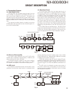
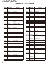
CIRCUIT DESCRIPTION
Loop
Filter
BUFF
AMP
BUFF
AMP
LPF
Ripple
Filter
VCO
150C
VC
TCXO
PLL
IC3 Q9
Q5,Q6
D3,D4
D7~D12,D14
BUFF
AMP
Q10
Q3
SDO1
SCK1
/PCS RF
X1
19.2MHz
T/R
SW
D101,D205
50C
50C
to TX stage
80T
50R
to Local Amplifier
IC5
Q1
IC4
CV
VCO MOD
ASSIST
Fig. 7