


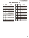
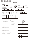
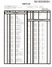
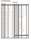
NX-800/800H
21
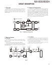
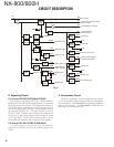
6. Control Circuit
The control circuit consists of MCU (IC510) and its pe-
ripheral circuits. IC510 mainly performs the following;
1) Switching between transmission and reception by PTT
signal input.
2) Reading system, zone, frequency, and program data
from the memory circuit.
3) Sending frequency program data to the PLL.
4) Controlling squelch on/off by the DC voltage from the
squelch circuit.
5) Controlling the audio mute circuit by decode data input.
6-1. MCU
The MCU (IC510) is 32bit RISC processor, equipped with
peripheral function and ADC/DAC.
This MCU operates at 18.432MHz clock and 3.3V /1.5V
DC. Controls the flash memory, SRAM, DSP, the receive
circuit, the transmitter circuit, the control circuit, and the dis-
play circuit and transfers data to or from an external device.
6-2. Memory Circuit
Memory circuit consists of the MCU (IC510) and the
SRAM (IC503), the fl ash memory (IC501). The fl ash memo-
ry has capacity of 32Mbit that contains the transceiver con-
trol program for the MCU and stores the data. It also stores
the data for transceiver channels and operating parameter
that are written by the FPU. This program can be easily
written from external devices. The SRAM has capacity of
1Mbit that contains work area and data area.
■
Flash memory
Note: The fl ash memory stores the data that is written
by the FPU (KPG-111D), tuning data (Deviation, Squelch,
etc.), and fi rmware program.
■
SRAM (static memory)
Note: The SRAM has temporary data area and work
area.
When the power supply is off, it is backed up by an inter-
nal secondary lithium battery. Therefore, the save data does
not break.
■
Real-time clock
The clock function is based on real-time clock IC (IC504).
When the power supply is off, it is backed up by an internal
secondary lithium battery
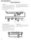
6-3. Display Unit
The display unit is composed of the MCU (IC911) and
the memory IC (IC913), and the LCD & Key backlight etc.
The LCD Ass’y (with LCD Driver) is controlled using the
bus lines on the connector (CN905) of the display unit. It
corrects the LCD contrast voltage using IC909.
6-4. Key Detection Circuit
Keys are detected using Key scan circuit in IC911. The
/KI* and KO* signals that are normally pulled up go low
when any key is pressed.
6-5. DSP
The DSP circuit consists of a DSP (IC502) and processes
the base band signal. The DSP operates on an external
clock of 18.432MHz (the same as the IC510), the I/O sec-
tion operates at 3.3V and the core section operates at 1.5V.
The DSP carries out the following processes:
• 4Level FSK processing
• Analog FM pre-emphasis/de-emphasis
• Vocoder processing between audio codec and modula-
tion/demodulation
• CAI processing, such as error correction encoding
• QT/DQT encoding/decoding
• DTMF encoding/decoding
• MSK encoding/decoding
• 2TONE encoding/decoding
• Compressor/expander processing
• Voice scrambler processing
• Transmit/receive audio fi ltering processing
• Microphone amplifi er AGC processing
• Audio mute processing
• Modulation level processing
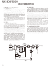
7. Power Supply Circuit
+B is connected to Final amplifi er and DC/DC converter
IC (IC405). IC405 regulates +B voltage to 5.0V (50M). 50M
operates whenever +B is supplied. IC402 (33M), IC408 (33A)
and IC409 (15M) are enabled while the 50M are operating.
33M and 15M provide the power to MCU, DSP, and
Flash memory. At this time MCU starts working. Voltage
detector IC (IC401) watches +B voltage. If +B voltage is
higher than 8.6V, IC401 (/BINT) outputs High. If the /BINT
signal is high, Q404 (SB SW) is turned on by SBC signal
from MCU. (High: SB=ON, Low: SB=OFF). When the SB
is turned on, IC403 (80C), IC404 (50C), IC406 (33C), IC407
(33GPS) and IC410 (150C) start working. Q416 and Q412
are controlled by SBC signal. If the SBC signal becomes
High, Q416 (33A-2) operates and Q412 (50MC SW) are
turned on.
The MCU controls the TXC signal to High during trans-
mission to supply power (80T) for transmission circuit. The
MCU controls the signals (RXC) to High during reception to
supply power (80R, 50R) for reception circuit.
When the MCU detects the PSW (Power switch) signal,
IGN (Ignition sense) signal or /BINT signal, it controls the
SBC signal to Low, and turns the transceiver power (SB) off.
When D401 and Q401 detect over-voltage condition, they
turns Q404 (SB SW) off. But the MCU still works.
If +B is not provided to the transceiver, the power is pro-
vided to SRAM and RTC through the secondary battery con-
nected with CN405.
CIRCUIT DESCRIPTION