


3 - 23
3. SIGNALS AND WIRING
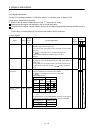
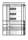
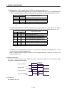
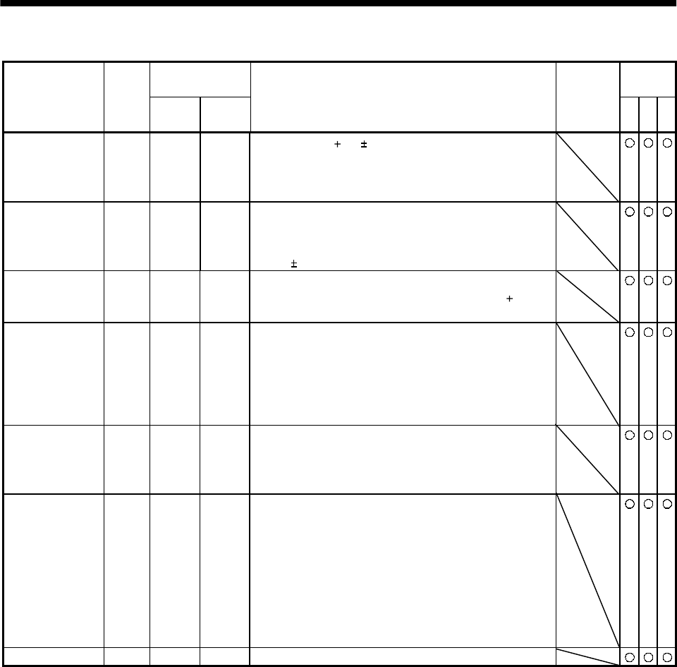
(4) Power supply
Connector pin No.
Control
mode
Signal Symbol
7kW or
less
11kW or
more
Functions/Applications I/O division
PST
I/F internal
power supply
VDD CN1B
3
CN1B
3
Used to output 24V 10% to across VDD-SG.
When using this power supply for digital interface,
connect it with COM.
Permissible current : 80mA
Digital I/F power
supply input
COM CN1A
9
CN1B
13
CN1A
9
CN1B
13
Used to input 24VDC for input interface.
Connect the positive terminal of the 24VDC external
power supply.
24VDC
10%
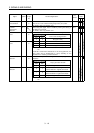
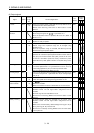
Open collector
power input
OPC CN1A
11
CN1A
11
When inputting a pulse train in the open collector
system, supply this terminal with the positive (
) power
of 24VDC.
Digital I/F
common
SG CN1A
10
20
CN1B
10
20
CN1A
10
20
CN1B
10
20
Common terminal for input signals such as SON and
EMG. Pins are connected internally.
Separated from LG.
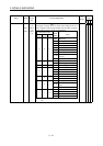
15VDC power
supply
P15R CN1A
4
CN1B
11
CN1A
4
CN1B
11
Outputs 15VDC to across P15R-LG. Available as power
for TC, TLA, VC, VLA.
Permissible current: 30mA
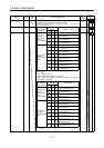
Control common LG CN1A
1
CN1B
1
CN3
1, 11
3, 13
CN1A
1
CN1B
1
CN3
1, 11
3, 13
CN4
4
Common terminal for TLA, TC, VC, VLA, FPA, FPB, OP
,MO1, MO2 and P15R.
Pins are connected internally.
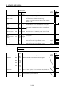
Shield SD Plate Plate Connect the external conductor of the shield cable.