


4-8
Chapter 4, FRONT AND REAR PANELS
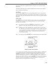
4.2.11 CH1, CH2 Connectors
The signal at these connectors is an analog voltage corresponding to a selected
output, such as X, Y, R, θ, etc., as specified in the Output Setup menu. The minimum
time constant that can be used is 5 ms. The full-scale output voltage range is ±10.0 V
although the outputs remain valid to ±12.0 V to provide some overload capability.
4.2.12 TRIG Connector
This connector accepts a TTL-compatible input and can be used for triggering the
auxiliary Analog to Digital Converters (ADCs). The input operates on the positive
edge only.
4.2.13 ADC1, ADC2 Connectors
The input voltages at these connectors may be digitized using the auxiliary ADCs and
read either from the front panel or by the use of a computer interface command. The
input voltages are sampled and held when the ADC is triggered, and several different
trigger modes are available. These modes can be set either from the front panel or by
using a remote computer command. The input voltage range is ±10.0 V and the
resolution is 1 mV.
4.2.14 DAC1, DAC2 Connectors
There are two DAC (Digital to Analog Converter) output connectors. The output
voltages at these connectors can be set either from the front panel or by the use of
remote computer commands. The output range is ±10.0 V and the resolution is 1 mV.
4.2.15 FAST X, FAST Y Connectors
The signals at these two connectors are the X channel and Y channel output signals
derived from a point after the first stage of output low-pass filtering. The maximum
time constant that can be used is 640 µs, with a fixed slope of 6 dB/octave. Visual
interpretation of the waveforms at these connectors, as displayed on an oscilloscope,
when the instrument is operating in the highband mode (i.e. above 60 kHz) is
difficult.