


WFM90D and WFM91D Service Manual
3-1
Theory of Operation
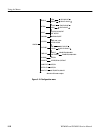
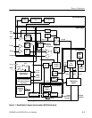
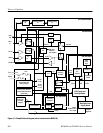
This section contains a module-level description of the instrument circuitry. The
description is based on the block diagram in Figure 3--1. (For serial numbers
below B020100, see Figure 3--2).
Input Board
The signal input and output connectors are located on the Input board. There are
receivers for the Audio, Video, and External Reference inputs. This board also
provides an automatic equalizer for serial digital video inputs, a switch for the
video signal reference, and a variable gain circuit for the audio input.
The output of the serial digital video automatic equalizer is routed to the SDI
Interface board for further processing and a video signal is returned from the SDI
Interface board. A signal line, DIG, from the SDI Interface board can disable the
video input amplifier to select the video signal from the SDI Interface board or it
can disable the video from the SDI Interface board and enable the video from the
video input amplifier.
The video input signal has a DC voltage feedback clamp from the Bottom board.
The video output signal from the Bottom board is routed through the Input
board. The audio variable gain is controlled by the microprocessor serial bus,
which is routed to the Input board from the Top board through the Bottom board.
SDI Interface Board
The equalized SDI signal from the Input board is received on the SDI and
N_SDI lines. A clock extraction and reclocking function provides clock and data
on the SDOP, SDON, SCOP, SCON lines. It also provides the “LOCK” output,
which determines whether an SDI signal is present. This board also provides a
serial-to-parallel function, as well as system detection and EDH functionality.
The parallel data and clock are then fed to a digital-to-analog converter with
composite encoding functions. The output of the converter is filtered and
amplified before being sent to the Input B oard.
The video output amplifier can be disabled by a low on the DIG line to allow for
an analog input to the Input board. An A/D converter measures the voltage on
the CARRIER_DET line to estimate the degradation that the SDI signal has
experienced due to long cables and so forth.
The entire board is controlled by a I2C bus with the I2C clock on SCLK and the
I2C data on MOSI.