


PLL/Clock
Generator
Power
Management
Pin
Multiplexing
JTAG Interface
64 KB DARAM
256 KB SARAM
128 KB ROM
Switched Central Resource (SCR)
Input
Clock(s)
FFT Hardware
Accelerator
C55x™ DSP CPU
DSP System
LCD
Bridge
Display
I S
(x4)
2
I C
2
SPI
UART
Serial Interfaces
10-Bit
SAR
ADC
App-Spec
USB 2.0
PHY (HS)
[DEVICE]
Connectivity
Peripherals
DMA
(x4)
Interconnect
NAND, NOR,
SRAM, mSDRAM
Program/Data Storage
MMC/SD
(x2)
System
GP Timer
(x2)
RTC
GP Timer
or WD
LDOs
Chapter 1
SPRUFX5A–October 2010–Revised November 2010
System Control
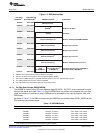
1.1 Introduction
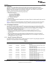
The TMS320C5515 digital signal processor (DSP) contains a high-performance, low-power DSP to
efficiently handle tasks required by portable audio, wireless audio devices, industrial controls, software
defined radio, fingerprint biometrics, and medical applications. The C5515 DSP consists of the following
primary components:
• A C55x CPU and associated memory
• FFT hardware accelerator
• Four DMA controllers and external memory interface
• Power management module
• A set of I/O peripherals that includes I2S, I2C, SPI, UART, Timers, EMIF, 10-bit SAR ADC, LCD
Controller, USB 2.0
For more information on these components see the following documents:
• TMS320C55x 3.0 CPU Reference Guide (SWPU073).
• TMS320C55x DSP Peripherals Overview Reference Guide (SPRU317).
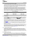
1.1.1 Block Diagram
The C5515 DSP block diagram is shown in Figure 1-1 .
Figure 1-1. Functional Block Diagram
13
SPRUFX5A–October 2010–Revised November 2010 System Control
Submit Documentation Feedback
Copyright © 2010, Texas Instruments Incorporated