


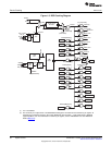
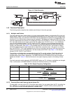
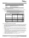
CLKREF
Reference
Divider
1
0
CGCR2[RDBYPASS]
PLL
LS
PLLIN
PLLOUT
Output
Divider
0
CGCR4.
[OUTDIVEN]
1
0
CCR2.
[SYSCLKSEL]
LS
SYSCLK
CLKSEL
1
0
CLKIN
RTC Clock
LS
RTC
OSC
RTC_XI
RTC_XO
32.768
KHz
RTC_CLKOUT
RTC
1
( )
M + 4
CLKREF
RDRATIO + 4
´
( )
M + 4
1
CLKREF
RDRATIO + 4 ODRATIO + 1
´ ´
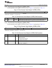
CLKREF
M + 4
´
é ù
ë û
1
CLKREF
M + 4
ODRATIO + 1
´ ´
é ù
ë û
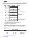
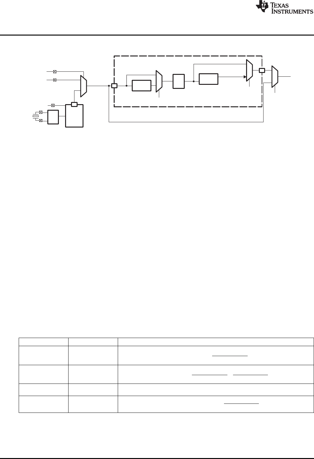
System Clock Generator
www.ti.com
Figure 1-4. Clock Generator
1.4.2 Functional Description
The following sections describe the multiplier and dividers of the clock generator.
1.4.2.1 Multiplier and Dividers
The clock generator has a one multiplier and a two programmable dividers: one before the PLL input and
one on the PLL output. The PLL can be programmed to multiply the PLL input clock, PLLIN, using a x4 to
x4099 multiplier value. The reference clock divider can be programmed to divide the clock generator input
clock from a /4 to /4099 divider ratio and may be bypassed. The Reference Divider and RDBYPASS mux
must be programmed such that the PLLIN frequency range is 32.786 KHz to 170 KHz. At the output of the
PLL, the output divider can be used to divide the PLL output clock, PLLOUT, from a /1 to a /128 divider
ratio and may also be bypassed. The PLL output, PLLOUT, frequency must be programmed within the
range of at least 60 MHz and no more than the maximum operating frequency defined by the datasheet,
Fsysclk_max parameter. See Table 1-10 for allowed values of PLLIN, PLLOUT, and SYSCLK. Keep in
mind that programming the output divider with an odd divisor value other than 1 will result in a non-50%
duty cycle SYSCLK. This is not a problem for any of the on-chip logic, but the non-50% duty cycle will be
visible on chip pins such as EM_SDCLK (in full-rate mode) and CLKOUT. See Table 1-10 for allowed
values of PLLIN, PLLOUT, and SYSCLK.
The multiplier and divider ratios are controlled through the PLL control registers. The M bits define the
multiplier rate. The RDRATIO and ODRATIO bits define the divide ratio of the reference divider and
programmable output divider, respectively. The RDBYPASS and OUTDIVEN bits are used to enable or
bypass the dividers. Table 1-5 lists the formulas for the output frequency based on the setting of these
bits.
The clock generator must be placed in BYPASS MODE when any PLL dividers or multipliers are changed.
Then, it must remain in BYPASS MODE for at least 4 mS before switching to PLL MODE.
Table 1-5. PLL Output Frequency Configuration
RDBYPASS OUTDIVEN SYSCLK Frequency
0 0
0 1
1 0
1 1
1.4.2.2 Powering Down and Powering Up the System PLL
To save power, you can put the PLL in its power down mode. You can power down the PLL by setting the
PLL_PWRDN = 1 in the clock generator control register CGCR1. However, before powering down the
PLL, you must first place the clock generator in bypass mode.
24
System Control SPRUFX5A–October 2010–Revised November 2010
Submit Documentation Feedback
Copyright © 2010, Texas Instruments Incorporated