


www.ti.com
System Clock Generator
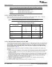
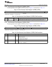
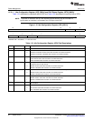
1.4.4.3 Clock Generator Control Register 3 (CGCR3) [1C22h]
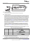
The clock generator control register 3 (CGCR3) is shown in Figure 1-8 and described in Table 1-15.
Figure 1-8. Clock Generator Control Register 3 (CGCR3) [1C22h]
15 0
INIT
R/W-0806h
LEGEND: R/W = Read/Write; -n = value after reset
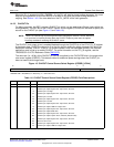
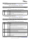
Table 1-15. Clock Generator Control Register 3 (CGCR3) Field Descriptions
Bit Field Value Description
15-0 INIT 0x0806h Initialization bits for the DSP clock generator. These bits are used for testing purposes and
must be initialized with 0x806 during PLL configuration for proper operation of the PLL.
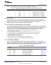
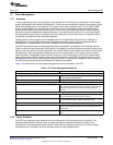
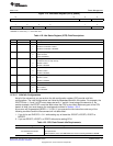
1.4.4.4 Clock Generator Control Register 4 (CGCR4) [1C23h]
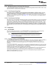
The clock generator control register 4 (CGCR4) is shown in Figure 1-9 and described in Table 1-16.
Figure 1-9. Clock Generator Control Register 4 (CGCR4) [1C23h]
15 10 9 8 7 0
Reserved OUTDIVEN Reserved ODRATIO
R-0 R/W-0 R-0 R/W-0
LEGEND: R/W = Read/Write; R = Read only; -n = value after reset
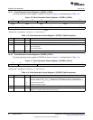
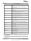
Table 1-16. Clock Generator Control Register 4 (CGCR4) Field Descriptions
Bit Field Value Description
15-10 Reserved 0 Reserved.
9 OUTDIVEN Output divider enable bit. This bit determines whether the output divider of the PLL is are
enabled or bypassed.
0 The output divider is bypassed.
1 The output divider is enabled.
8 Reserved 0 Reserved.
7-0 ODRATIO 0-FFh Divider ratio bits for the output divider of the PLL.
Divider value = ODRATIO + 1.
31
SPRUFX5A–October 2010–Revised November 2010 System Control
Submit Documentation Feedback
Copyright © 2010, Texas Instruments Incorporated