


Device Clocking
www.ti.com
pins for the load mode register command. During the mobile SDRAM initialization, the device issues the
load mode register initialization command to two different addresses that differ in only the BA0 and BA1
address bits. These registers are the Extended Mode register and the Mode register. The extended mode
register exists only in mSDRAM, and not in non-mSDRAM. If a non-mobile SDRAM memory ignores bits
BA0 and BA1, the second loaded register value overwrites the first, leaving the desired value in the mode
register and the non-mobile SDRAM works with the device.
Some timing parameters are programmable such as the refresh rate and CAS latencies. The EMIF
supports up to 100 MHz SDCLK and has the ability to run the SDCLK at half the system clock to meet the
EMIF I/O timing requirements and/or at lower power if a slower SDCLK can be used. Detailed information
is available in the Clock Control section of the TMS320C5515/14/05/04 DSP External Memory Interface
(EMIF) User's Guide (SPRUGU6).
1.2.2 I/O Memory Map
The C5x DSP has a separate memory map for peripheral and system registers, called I/O space. This
space is 64K-words in length and is accessed via word read and write instructions dedicated for I/O
space.
Separate documentation for I/O space registers related to each peripheral exists and is listed in the
preface of this guide. System registers, which provide system-level control and status, are described in
detail in other sections throughout this guide. Unused addresses in I/O space should be treated as
reserved and should not be accessed. Accessing unused I/O space addresses may stall or hang the DSP.
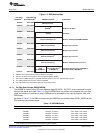
Each of the four DMA controllers has access to a different set of peripherals and their I/O space registers.
This is shown in Section 1.7.4.
NOTE: Writting to I/O space registers incurs in at least 2 CPU cycle latency. Thus, when
configuring peripheral devices, wait at least two cycles before accessing data from the
peripheral. When more than one peripheral register is updated in a sequence, the CPU only
needs to wait following the final register write. For example, if the EMIF is being
reconfigured, the CPU must wait until the very last EMIF register update takes effect before
trying to access the external memory. The users should consult the respective peripheral
user's guide to determine if a peripheral requires additional initialization time.
Before accessing any peripheral register, make sure the peripheral is not held in reset and its internal
clock is enabled. The peripheral reset control register (Section 1.7.5.2) and the peripheral clock gating
control registers (Section 1.5.3.2.1) control these functions. Accessing a peripheral whose clocks are
gated will either return the value of the last address read from the peripheral (when the clocks were last
ON) or it may possibly hang the DSP -- depending on the peripheral.
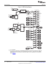
1.3 Device Clocking
1.3.1 Overview
The DSP requires two primary reference clocks: a system reference clock and a USB reference clock. The
system clock, which is used by the CPU and most of the DSP peripherals, is controlled by the system
clock generator. The system clock generator features a software-programmable PLL multiplier and several
dividers. The system clock generator accepts an input reference clock from the CLKIN pin or the output
clock of the 32.768-KHz real-time clock (RTC) oscillator. The selection of the input reference clock is
based on the state of the CLK_SEL pin. The CLK_SEL pin is required to be statically tied high or low and
cannot change dynamically after reset. The system clock generator can be used to modify the system
reference clock signal according to software-programmable multiplier and dividers. The resulting clock
output, the DSP system clock, is passed to the CPU, peripherals, and other modules inside the DSP.
Alternatively, the system clock generator can be fully bypassed and the input reference clock can be
passed directly to the DSP system clock. The USB reference clock is generated using a dedicated on-chip
oscillator with a 12 MHz external crystal connected to the USB_MXI and USB_MXO pins. This crystal is
not required if the USB peripheral is not being used. The USB oscillator cannot be used to provide the
system reference clock.
The RTC oscillator generates a clock when a 32.768-KHz crystal is connected to the RTC_XI and
20
System Control SPRUFX5A–October 2010–Revised November 2010
Submit Documentation Feedback
Copyright © 2010, Texas Instruments Incorporated