


www.ti.com
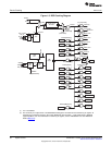
System Clock Generator
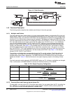
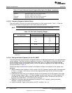
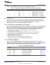
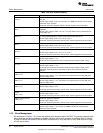
Table 1-11 shows programming examples for different PLL MODE frequencies.
Table 1-11. Examples of Selecting a PLL MODE Frequency, When CLK_SEL=L
RDBYPASS OUTDIVEN M RDRATIO ODRATIO PLL Output Frequency
1 0 173h X X 32.768KHz x (173h+4) = 12.288 MHz
1 1 E4Ah X 2 32.768KHz x (E4Ah + 4)/3 = 40.00 MHz
1 0 723h X X 32.768KHz x (723h + 4) = 60.00 MHz
1 0 8EDh X X 32.768KHz x (8EDh + 4) = 75.01 MHz
1 0 BE8h X X 32.768KHz x (BE7h + 4) = 100.01 MHz
1 0 E4Ah X X 32.768KHz x (E4Ah + 4) = 120.00 MHz
1.4.3.2.5 Lock Time
As previously discussed, you must place the clock generator in bypass mode before changing the PLL
settings. The time it takes the PLL to complete its phase-locking sequence is referred to as the lock time.
The PLL has a lock time of 4 ms. Software is responsible for ensuring the PLL remains in
BYPASS_MODE for at least 4 ms before switching to PLL_MODE.
1.4.3.2.6 Software Steps To Modify Multiplier and Divider Ratios
You can follow the steps below to program the PLL of the DSP clock generator. The recommendation is to
stop all peripheral operation before changing the PLL frequency, with the exception of the device CPU and
USB. The device CPU must be operational to program the PLL controller. Software is responsible for
ensuring the PLL remains in BYPASS_MODE for at least 4 ms before switching to PLL_MODE.
1. Make sure the clock generator is in BYPASS MODE by setting SYSCLKSEL = 0.
2. Set CLR_CNTL = 0 in CGCR1.
3. Program RDRATIO, M, and RDBYPASS in CGCR2 according to your required settings.
4. Program ODRATIO and OUTDIVEN in CGCR4 according to your required settings.
5. Write 0806h to the INIT field of CGCR3.
6. Set PLL_PWRDN = 0, CLR_CNTL = 1.
7. Wait 4 ms for the PLL to complete its phase-locking sequence.
8. Place the clock generator in its PLL MODE by setting SYSCLKSEL = 1.
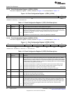
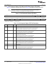
1.4.4 Clock Generator Registers
Table 1-12 lists the registers associated with the clock generator of the DSP. The clock generator
registers can be accessed by the CPU at the 16-bit addresses specified in Table 1-12. Note that the CPU
accesses all peripheral registers through its I/O space. All other register addresses not listed in Table 1-12
should be considered as reserved locations and the register contents should not be modified.
Table 1-12. Clock Generator Registers
CPU Word Acronym Register Description Section
Address
1C20h CGCR1 Clock Generator Control Register 1 Section 1.4.4.1
1C21h CGCR2 Clock Generator Control Register 2 Section 1.4.4.2
1C22h CGCR3 Clock Generator Control Register 3 Section 1.4.4.3
1C23h CGCR4 Clock Generator Control Register 4 Section 1.4.4.4
1C1Eh CCR1 Clock Configuration Register 1 Section 1.4.4.5
1C1Fh CCR2 Clock Configuration Register 2 Section 1.4.4.6
29
SPRUFX5A–October 2010–Revised November 2010 System Control
Submit Documentation Feedback
Copyright © 2010, Texas Instruments Incorporated