


www.ti.com
System Configuration and Control
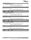
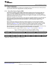
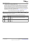
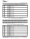
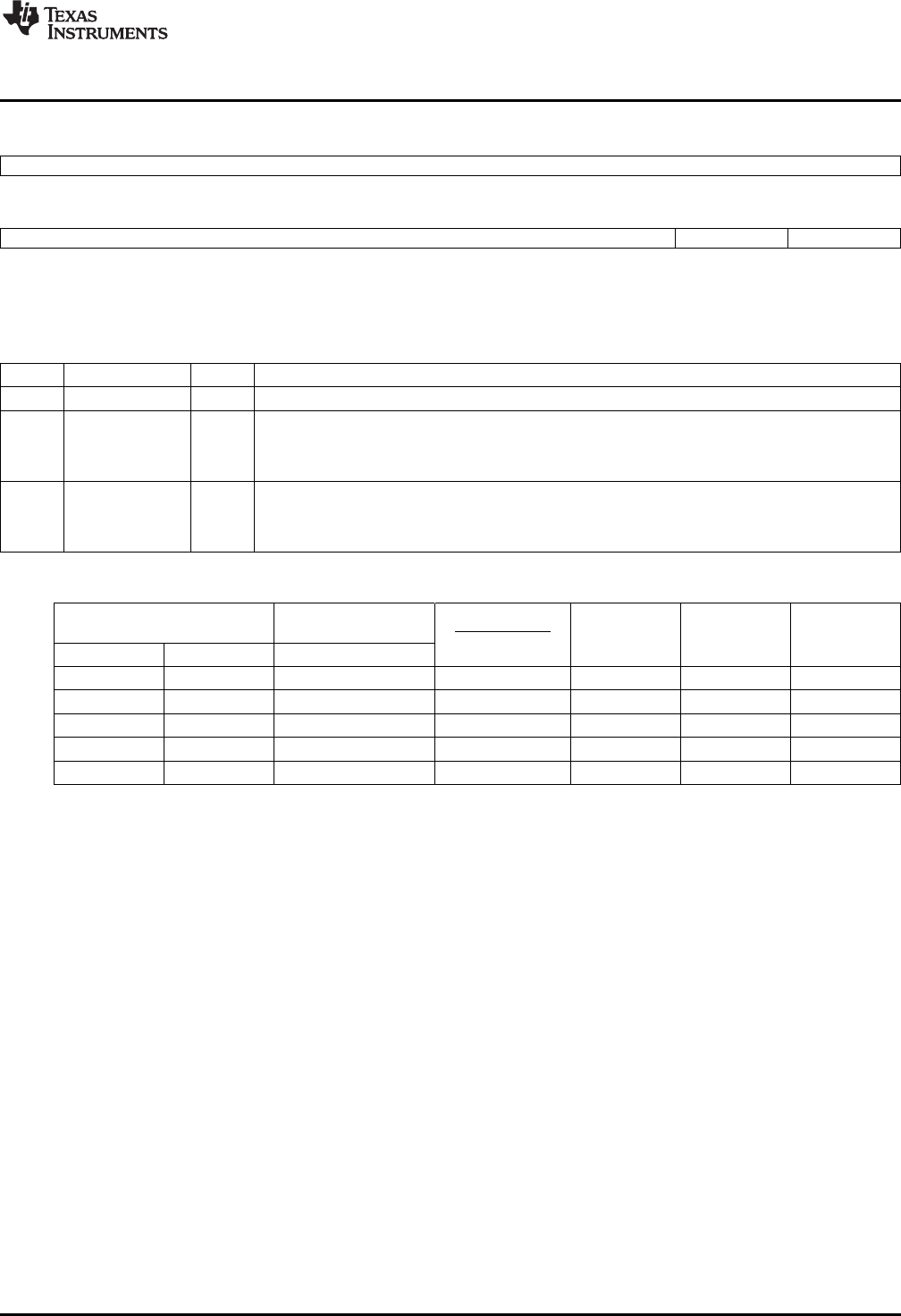
Figure 1-37. LDO Control Register (LDOCNTL) [7004h]
15 8
Reserved
R-0
7 2 1 0
Reserved DSP_LDO_V USB_LDO_EN
R-0 R/W-0 R/W-0
LEGEND: R/W = Read/Write; R = Read only; -n = value after reset
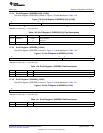
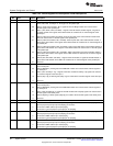
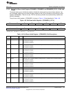
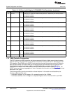
Table 1-46. LDOCNTL Register Bit Descriptions Field Descriptions
Bit Field Value Description
15-2 Reserved 0 Reserved. Read-only, writes have no effect.
1 DSP_LDO_V DSP_LDO voltage select bit.
0 DSP_LDOO is regulated to 1.3 V.
1 DSP_LDOO is regulated to 1.05 V.
0 USB_LDO_EN USB_LDO enable bit.
0 USB_LDO output is disabled. USB_LDOO pin is placed in high-impedance (Hi-Z) state.
1 USB_LDO output is enabled. USB_LDOO is regulated to 1.3 V.
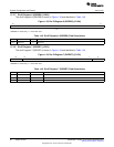
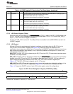
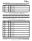
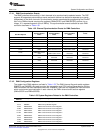
Table 1-47. LDO Controls Matrix
RTCPMGT Register LDOCNTL Register
(0x1930) (0x7004)
DSP_LDO_EN
BG_PD Bit LDO_PD Bit USB_LDO_EN Bit (Pin D12) ANA_LDO DSP_LDO USB_LDO
1 Don't Care Don't Care Don't Care OFF OFF OFF
Don't Care 1 Don't Care Don't Care OFF OFF OFF
0 0 0 Low ON ON OFF
0 0 0 High ON OFF OFF
0 0 1 Low ON ON ON
65
SPRUFX5A–October 2010–Revised November 2010 System Control
Submit Documentation Feedback
Copyright © 2010, Texas Instruments Incorporated