


Power Management
www.ti.com
1.5.3.4.1 Clock Configuration Process
The clock configuration process for the USB clock domain consists of disabling the USB peripheral clock
followed by disabling the USB on-chip oscillator. This procedure will completely shut off USB module,
which does not comply with USB suspend/resume protocol.
To set the clock configuration of the USB clock domain to idle follow these steps:
1. Set the SUSPENDM bit in FADDR register. For more information about the SUSPENDM bit, see the
TMS320C5515/14/05/04 DSP Universal Serial Bus 2.0 (USB) Controller User's Guide (SPRUGH9).
2. Set the USB clock stop request bit (USBCLKSTREQ) in the CLKSTOP register to request permission
to shut off the USB peripheral clock.
3. Wait until the USB acknowledges the clock stop request by polling the USB clock stop acknowledge bit
(USBCLKSTPACK) in the CLKSTOP register.
4. Disable the USB peripheral clock by setting USBCG = 1 in the peripheral clock gating control register 2
(PCGCR2).
5. Disable the USB oscillator by setting USBOSCDIS = 1 in the USB system control register (USBSCR).
To enable the USB clock domain, follow these steps:
1. Enable the USB oscillator by setting USBOSCDIS = 0 in USBSCR.
2. Wait for the oscillator to stabilize. Refer to the device-specific data manual for oscillator stabilization
time.
3. Enable the USB peripheral clock by setting USBCG = 0 in the peripheral clock gating control register 2
(PCGCR2).
4. Clear the USB clock stop request bit (USBCLKSTREQ) in the CLKSTOP register.
5. Clear the SUSPENDM bit in FADDR register.
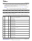
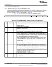
1.5.3.4.2 USB System Control Register (USBSCR) [1C32h]
The USB system control register is used to disable the USB on-chip oscillator and to power-down the
USB.
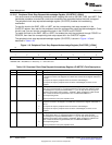
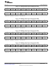
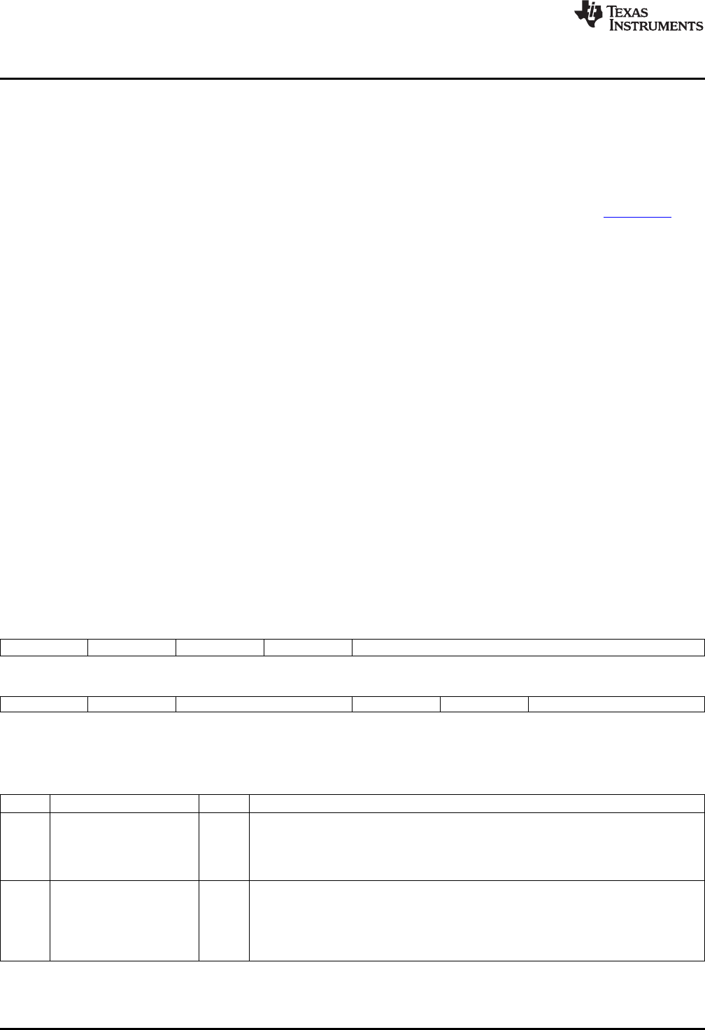
The USB system control register (USBSCR) is shown in Figure 1-17 and described in Table 1-27.
Figure 1-17. USB System Control Register (USBSCR) [1C32h]
15 14 13 12 11 8
USBPWDN USBSESSEND USBVBUSDET USBPLLEN Reserved
R/W-1 R/W-0 R/W-1 R/W-0 R-0
7 6 5 4 3 2 1 0
Reserved USBDATPOL Reserved USBOSCBIASDIS USBOSCDIS BYTEMODE
R-0 R/W-1 R-0 R/W-1 R/W-1 R/W-0
LEGEND: R/W = Read/Write; R = Read only; -n = value after reset
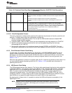
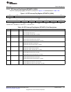
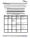
Table 1-27. USB System Control Register (USBSCR) Field Descriptions
Bit Field Value Description
15 USBPWDN USB module power. Asserting USBPWDN puts the USB PHY and PLL in their lowest
power state. The USB peripheral is not operational in this state.
0 USB module is powered.
1 USB module is powered-down.
14 USBSESSEND USB VBUS session end comparator enable. The USB VBUS pin has two comparators
that monitor the voltage level on the pin. These comparators can be disabled for power
savings when not needed.
0 USB VBUS session end comparator is disabled.
1 USB VBUS session end comparator is enabled.
44
System Control SPRUFX5A–October 2010–Revised November 2010
Submit Documentation Feedback
Copyright © 2010, Texas Instruments Incorporated