


www.ti.com
System Configuration and Control
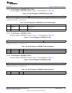
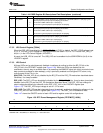
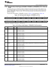
Table 1-44. EBSR Register Bit Descriptions Field Descriptions (continued)
Bit Field Value Description
2 A17_MODE A17 Pin Mode Bit. This bit controls the pin multiplexing of the EMIF address 17 (EM_A[17]) and
general-purpose input/output pin 23 (GP[23]) pin functions.
0 Pin function is EMIF address pin 17 (EM_A[17]).
1 Pin function is general-purpose input/output pin 23 (GP[23]).
1 A16_MODE A16 Pin Mode Bit. This bit controls the pin multiplexing of the EMIF address 16 (EM_A[16]) and
general-purpose input/output pin 22 (GP[22]) pin functions.
0 Pin function is EMIF address pin 16 (EM_A[16]).
1 Pin function is general-purpose input/output pin 22 (GP[22]).
0 A15_MODE A15 Pin Mode Bit. This bit controls the pin multiplexing of the EMIF address 15 (EM_A[15]) and
general-purpose input/output pin 21 (GP[21]) pin functions.
0 Pin function is EMIF address pin 15 (EM_A[15]).
1 Pin function is general-purpose input/output pin 21 (GP[21]).
1.7.3.2 LDO Control Register [7004h]
When the DSP_LDO is enabled by the DSP_LDO_EN pin [D12], by default, the DSP_LDOO voltage is set
to 1.3 V. The DSP_LDOO voltage can be programmed to be either 1.05 V or 1.3 V via the DSP_LDO_V
bit (bit 1) in the LDO Control Register (LDOCNTL).
At reset, the USB_LDO is turned off. The USB_LDO can be enabled via the USBLDOEN bit (bit 0) in the
LDOCNTL register.
1.7.3.3 LDO Control
All three LDOs can be simultaneously disabled via software by writing to either the BG_PD bit or the
LDO_PD bit in the RTCPMGT register (see Figure 1-36). When the LDOs are disabled via this
mechanism, the only way to re-enable them is by asserting the WAKEUP signal pin (which must also have
been previously enabled to allow wakeup), or by a previously enabled and configured RTC alarm, or by
cycling power to the CV
DDRTC
pin.
ANA_LDO: The ANA_LDO is only disabled by the BG_PD and the LDO_PD mechanism described above.
Otherwise, it is always enabled.
DSP_LDO: The DSP_LDO can be statically disabled by the DSP_LDO_EN pin. It can be also dynamically
disabled via the BG_PD and the LDO_PD mechanism described above. The DSP_LDO can change its
output voltage dynamically by software via the DSP_LDO_V bit in the LDOCNTL register (see
Figure 1-37). The DSP_LDO output voltage is set to 1.3 V at reset.
USB_LDO: The USB_LDO can be independently and dynamically enabled or disabled by software via the
USB_LDO_EN bit in the LDOCNTL register (see Figure 1-37). The USB _LDO is disabled at reset.
Table 1-47 shows the ON/OFF control of each LDO and its register control bit configurations.
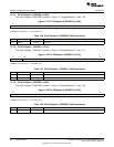
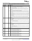
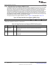
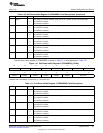
Figure 1-36. RTC Power Management Register (RTCPMGT) [1930h]
15 8
Reserved
R-0
7 5 4 3 2 1 0
Reserved WU_DOUT WU_DIR BG_PD LDO_PD RTCCLKOUTEN
R-0 R/W-0 R/W-0 R/W-0 R/W-0 R/W-0
LEGEND: R/W = Read/Write; R = Read only; -n = value after reset
63
SPRUFX5A–October 2010–Revised November 2010 System Control
Submit Documentation Feedback
Copyright © 2010, Texas Instruments Incorporated