


Power Management
www.ti.com
1.5.4 Static Power Management
1.5.4.1 RTC Power Management Register (RTCPMGT) [1930h]
This register enables static power management with power down and wake up register bits as described
in the device-specific data sheet and, more generally, below. The RTC power management register
(RTCPMGT) is shown in Figure 1-18 and described in Table 1-28.
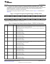
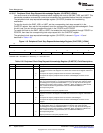
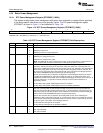
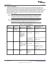
Figure 1-18. RTC Power Management Register (RTCPMGT) [1930h]
15 5 4 3 2 1 0
Reserved WU_DOUT WU_DIR BG_PD LDO_PD RTCCLKOUTEN
R-0 RW-0 RW-0 RW-0 RW-0 RW-0
LEGEND: R/W = Read/Write; R = Read only; -n = value after reset
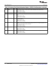
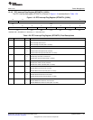
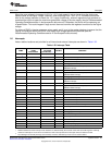
Table 1-28. RTC Power Management Register (RTCPMGT) Field Descriptions
Bit Field Value Description
15-5 Reserved 0 Reserved
4 WU_DOUT Wakeup output, active low/Open-drain.
0 WAKEUP pin driven low.
1 WAKEUP pin driver is in high impedance.
3 WU_DIR Wakeup pin direction control.
0 WAKEUP pin is configured as input.
1 WAKEUP pin is configured as output.
NOTE: The WAKEUP pin, when configured as an input, is active high. When it is configured as an
output, it is open-drain and thus it should have an external pull-up and it is active low.
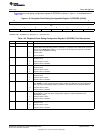
2 BG_PD Powerdown control bit for the bandgap, on-chip LDOs, and the analog POR (power on reset)
comparator. This bit shuts down the on-chip LDOs (ANA_LDO, DSP_LDO, and USB_LDO), the
Analog POR, and Bandgap reference. BG_PD and LDO_PD are only intended to be used when the
internal LDOs supply power to the chip. If the internal LDOs are bypassed and not used then the
BG_PD and LDO_PD power down mechanisms should not be used since the POR gets powered
down and the POWERGOOD signal would not get generated properly.
After this bit is asserted, the on-chip LDOs, Analog POR, and the Bandgap reference can only be
re-enabled by the WAKEUP pin (being driven HIGH externally) or an enabled RTC alarm or an
enabled RTC periodic event interrupt. Once reenabled, the Bandgap circuit takes about 100 msec to
charge the external 0.1 mF capacitor on the BG_CAP pin via the the internal resistance of
aproxmiately. 320 kΩ.
0 On-chip LDOs, Analog POR, and Bandgap reference are enabled.
1 On-chip LDOs, Analog POR, and Bandgap reference are disabled (shutdown).
1 LDO_PD On-chip LDOs and Analog POR power down bit. This bit shuts down the on-chip LDOs (ANA_LDO,
DSP_LDO, and USB_LDO) and the Analog POR. BG_PD and LDO_PD are only intended to be
used when the internal LDOs supply power to the chip. If the internal LDOs are bypassed and not
used then the BG_PD and LDO_PD power down mechanisms should not be used since POR gets
powered down and the POWERGOOD signal is not generated properly.
After this bit is asserted, the on-chip LDOs and Analog POR can only be re-enabled by the
WAKEUP pin (being driven HIGH externally) or an enabled RTC alarm or an enabled RTC periodic
event interrupt. This bit keeps the Bandgap reference turned on to allow a faster wake-up time with
the expense power consumption of the Bandgap reference.
0 On-chip LDOs and Analog POR are enabled.
1 On-chip LDOs and Analog POR are disabled (shutdown).
0 RTCCLKOUTEN Clock-out output enable.
0 Clock output disabled.
1 Clock output enabled.
46
System Control SPRUFX5A–October 2010–Revised November 2010
Submit Documentation Feedback
Copyright © 2010, Texas Instruments Incorporated