


Power Management
www.ti.com
1.5.4.3 Internal Memory Low Power Modes
To save power, software can place on-chip memory (DARAM or SARAM) in one of two power modes:
memory retention mode and active mode. These power modes are activated through the SLPZVDD and
SLPZVSS bits of the RAM Sleep Mode Control Register 1-5 (RAMSLPMDCNTLR[1:5]). To activate
memory retention mode, set SLPZVDD bit and clear SLPZVSS bit of each memory bank to be put in
retention mode. The retention/active mode of each 4kW DARAM and SARAM bank is independently
controllable.
When either type of memory is placed in memory retention, read and write accesses are not allowed. In
memory retention mode, the memory is placed in a low power mode while maintaining its contents. The
contents are retained as long as there are no access attempts to that memory. In active mode, the
memory is readily accessible by the CPU, but consumes more leakage power.
For the entire duration that the memory is in retention mode, there can be no attempts to read or write to
the memories address range. This includes accesses by the CPU or any DMA. If an access is attempted
while in retention mode then the memory contents will be lost.
NOTE: You must wait at least 10 CPU clock cycles after taking memory out of a low power mode
before initiating any read or write access.
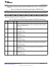
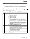
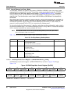
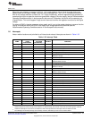
Table 1-30 summarizes the power modes for both DARAM and SARAM.
Table 1-30. On-Chip Memory Standby Modes
SLPZVDD SLPZVSS Mode CV
DD
Voltage
1 1 Active 1.05 V or 1.3 V
- Normal operational mode
- Read and write accesses are allowed
1 0 Retention 1.05 V or 1.3 V
- Low power mode
- Contents are retained
- No read or write access is allowed
0 0 Memory Disabled Mode 1.05 V or 1.3 V
- Lowest leakage mode
- Contents are lost
- No read or write access is allowed
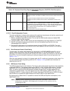
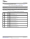
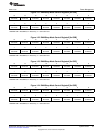
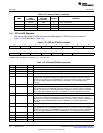
1.5.4.3.1 RAM Sleep Mode Control Register 1 (RAMSLPMDCNTLR1) [1C28h]
The RAM sleep mode control register 1 (RAMSLPMDCNTLR1) is shown in Figure 1-20 through
Figure 1-24.
Figure 1-20. RAM Sleep Mode Control Register1 [0x1C28]
15 14 13 12 11 10 9 8
DARAM7 DARAM7 DARAM6 DARAM6 DARAM5 DARAM5 DARAM4 DARAM4
SLPZVDD SLPZVSS SLPZVDD SLPZVSS SLPZVDD SLPZVSS SLPZVDD SLPZVSS
R/W+1 R/W+1 R/W+1 R/W+1 R/W+1 R/W+1 R/W+1 R/W+1
7 6 5 4 3 2 1 0
DARAM3 DARAM3 DARAM2 DARAM2 DARAM1 DARAM1 DARAM0 DARAM0
SLPZVDD SLPZVSS SLPZVDD SLPZVSS SLPZVDD SLPZVSS SLPZVDD SLPZVSS
R/W+1 R/W+1 R/W+1 R/W+1 R/W+1 R/W+1 R/W+1 R/W+1
LEGEND: R/W = Read/Write; R = Read only; -n = value after reset
48
System Control SPRUFX5A–October 2010–Revised November 2010
Submit Documentation Feedback
Copyright © 2010, Texas Instruments Incorporated