


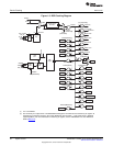

System Clock Generator
www.ti.com
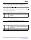
1.4.2.4 DSP Reset Conditions of the System Clock Generator
The following sections describe the operation of the system clock generator when the DSP is held in reset
state and the DSP is removed from its reset state.
1.4.2.4.1 Clock Generator During Reset
During reset, the PLL_PWRDN bit of the clock generator control register 1 (CGCR1) is set to 1, and the
PLL does not generate an output clock. Furthermore, the SYSCLKSEL bit of the clock configuration
register 2 (CCR2) defaults to 0 (BYPASS MODE), and the system clock (SYSCLK) is driven by either the
CLKIN pin or the real-time clock (RTC). See Section 1.4.3.1 for more information on the bypass mode of
the clock generator.
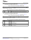
1.4.2.4.2 Clock Generator After Reset
After reset, the on-chip bootloader programs the system clock generator based on the input clock selected
via the CLK_SEL pin. If CLK_SEL = 0, the bootloader programs the system clock generator and sets the
system clock to 12.288 MHz (multiply the 32.768-kHz RTC oscillator clock by 375). If CLK_SEL = 1, the
bootloader bypasses the system clock generator altogether and the system clock is driven by the CLKIN
pin. In this case, the CLKIN frequency is expected to be 11.2896 MHz, 12.0 MHz, or 12.288 MHz. While
the bootloader tries to boot from the USB , the clock generator is programmed to output approximately 36
MHz.
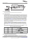
1.4.3 Configuration
1.4.3.1 BYPASS MODE
When the system clock generator is in the BYPASS MODE, the clock generator is not used and the
system clock (SYSCLK) is driven by either the CLKIN pin or the real-time clock (RTC).
NOTE: In bypass mode, the PLL is not automatically powered down and will still consume power.
For maximum power savings, the PLL should be placed in its power-down mode. See
Section 1.4.2.2 for more details.
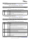
1.4.3.1.1 Entering and Exiting the BYPASS MODE
To enter the bypass mode, write a 0 to the SYSCLKSEL bit in the clock configuration register 2 (CCR2). In
bypass mode, the frequency of the system clock (SYSCLK) is determined by the CLK_SEL pin. If
CLK_SEL = 0, SYSCLK is driven by the output of the RTC. Otherwise, SYSCLK will be driven by the
CLKIN pin.
To exit the BYPASS MODE, ensure the PLL has completed its phase-locking sequence by waiting at least
4 ms and then write a 1 to the SYSCLKSEL bit. The frequency of SYSCLK will then be determined by the
multiplier and divider ratios of the PLL System Clock Generator.
If the clock generator is in the PLL MODE and you want to reprogram the PLL or any of the dividers, you
must set the clock generator to BYPASS MODE before changing the PLL and divider settings.
Logic within the clock generator ensures that there are no clock glitches during the transition from PLL
MODE to BYPASS MODE and vice versa.
26
System Control SPRUFX5A–October 2010–Revised November 2010
Submit Documentation Feedback
Copyright © 2010, Texas Instruments Incorporated