


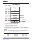
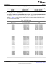
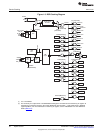
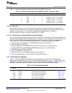

CLKSEL
1
0
CLKIN
PCGCR1
[SYSCLKDIS]
LS
1
0
LS
CCR2
[SYSCLKSEL]
SYSCLK
System Clock
Generator
ST3_55[CLKOFF]
CLKOUT
ICR[HWAI]
FFT Hardware
ICR[MPORTI]
MPORT Clock
ICR[XPORTI]
XPORT Clock
PCGCR2[DMA1CG]
DMA0
PCGCR2[DMA2CG]
DMA1
PCGCR2[DMA3CG]
DMA2
DMA3
ICR[IPORTI]
IPORT Clock
ICR[DPORTI]
DPORT Clock
ICR[CPUI]
CPU Clock
PCGCR1[EMIFCG]
÷2
0
1
ECDR[EDIV]
EMIF
PCGCR2[USBCG]
LS
USB
Digital
USB
OSC
USB_MXI
UDB_MXO
12 MHz
USBSCR
[USBOSCDIS]
PCGCR1[DMA0CG]
PCGCR1[SPICG]
SPI
PCGCR1[UARTCG]
I2C
PCGCR1[TMR2CG]
UART
PCGCR1[TMR1CG]
Timer2
Timer1
PCGCR1[I2CCG]
PCGCR1[TMR0CG]
Timer0
PCGCR1[I2S0CG]
I2S0
PCGCR1[I2S1CG]
I2S1
PCGCR1[I2S2CG]
I2S2
PCGCR1[I2S3CG]
I2S3
PCGCR2[SARCG]
SAR
PCGCR2[LCDCG]
LCD Controller
PCGCR1[MMCSD0CG]
MMC/SD0
PCGCR1[MMCSD1CG]
MMC/SD1
USBPHYCLK
RTC Clock
LS
RTC
OSC
RTC_XI
RTC_XO
32.768
KHz
RTC_CLKOUT
RTC
LS
CLKREF
(1)
(1) (1)
(1)
(2)
Accelerator
USB
PHY
60 MHz
USB
PLL
OFF
12 MHz
PCGCR2[ANAREGCG]
Analog
Registers
(1)
Device Clocking
www.ti.com
Figure 1-3. DSP Clocking Diagram
(1) LS = Level Shifter
(2) The CLKOUT pin's output driver is enabled/disabled through the CLKOFF bit of the CPU ST3_55 register. At
the beginning of the boot sequence, the on-chip Bootloader sets CLKOFF = 1 and CLKOUT pin is disabled
(high-impedance). For more information on the ST3_55 register, see the TMS320C55x 3.0 CPU Reference
Guide (SWPU073).
22
System Control SPRUFX5A–October 2010–Revised November 2010
Submit Documentation Feedback
Copyright © 2010, Texas Instruments Incorporated