


www.ti.com
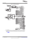
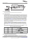
System Clock Generator
1.4.3.1.2 Register Bits Used in the BYPASS MODE
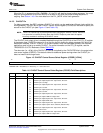
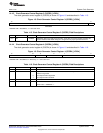
Table 1-7 describes the bits of the clock generator control registers that are used in the BYPASS MODE.
For detailed descriptions of these bits, see Section 1.4.4.
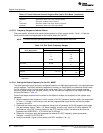
Table 1-7. Clock Generator Control Register Bits Used In BYPASS MODE
Register Bit Role in BYPASS MODE
SYSCLKSEL Allows you to switch to the PLL or BYPASS MODES.
PLL_PWRDN Allows you to power down the PLL.
1.4.3.1.3 Setting the System Clock Frequency In the BYPASS MODE
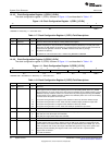
In the BYPASS MODE, the frequency of SYSCLK is determined by the CLK_SEL pin. If CLK_SEL = 0,
SYSCLK is driven by the output of the RTC. Otherwise, SYSCLK will be driven by the CLKIN pin.
NOTE: The CLK_SEL pin must be statically tied high or low; it cannot be changed after the device
has been powered up.
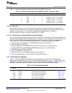
Table 1-8. Output Frequency in Bypass Mode
CLK_SEL SYSCLK Source / Frequency
1 CLKIN, expected to be one of the following values by the bootloader: 11.2896
MHz, 12.0MHz, or 12.288 MHz
0 RTC clock = 32.768 kHz
The state of the CLK_SEL pin is read via the CLKSELSTAT bit in the CCR2 register.
1.4.3.2 PLL MODE
In PLL MODE, the frequency of the input clock signal (CLKREF) can be both multiplied and divided to
produce the desired output frequency, and the output clock signal is phase-locked to the input clock
signal.
1.4.3.2.1 Entering and Exiting the PLL MODE
To enter the PLL_MODE from BYPASS_MODE, first program the PLL to the desired frequency. You must
always ensure the PLL has completed its phase-locking sequence before switching to PLL MODE. This
PLL has no lock indicator as such indicators are notoriously unreliable. Instead, a fixed amount of time
must be allowed to expire while in BYPASS_MODE to allow the PLL to lock. After 4 msec, write a 1 to the
SYSCLKSEL bit in the clock configuration register 2 (CCR2) to set the system clock to the output of the
PLL.
Whenever PLL needs to be reprogrammed, first the clock generator must be in bypass mode, and then
changed to PLL configuration. After waiting 4 msec, write a 1 to the SYSCLKSEL bit to get into the PLL
MODE.
Logic within the clock generator ensures that there are no clock glitches during the transition from
BYPASS MODE to PLL MODE and vice versa.
1.4.3.2.2 Register Bits Used in the PLL Mode
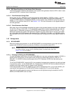
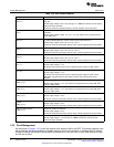
Table 1-9 describes the bits of the clock generator control registers that are used in the PLL MODE. For
detailed descriptions of these bits, see Section 1.4.4.
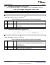
Table 1-9. Clock Generator Control Register Bits Used In PLL Mode
Register Bit Role in Bypass Mode
SYSCLKSEL Allows you to switch to the PLL or bypass modes.
RDBYPASS Determines whether reference divider should be bypassed or used.
27
SPRUFX5A–October 2010–Revised November 2010 System Control
Submit Documentation Feedback
Copyright © 2010, Texas Instruments Incorporated