Power Management
www.ti.com
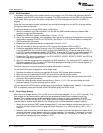
1.5.5.2 IDLE3 Procedure
In this power configuration all the power domains are turned on, the CPU and clock generator domains
are disabled, and the RTC clock domain is enabled. The DSP peripherals and the USB are also disabled
in this mode. When you enter this power configuration, all CPU and peripheral activity in the DSP is
stopped.
Since the clock generator domain is disabled, you must allow enough time for the PLL to re-lock before
exiting this power configuration.
Follow these steps to enter the IDLE3 power configuration:
1. Wait for completion of all DMA transfers. You can poll the DMA transfer status and disable DMA
transfers through the DMA registers.
2. Disable the USB clock domain as described in Section 1.5.3.4.
3. Idle all the desired peripherals in the peripheral clock domain by modifying the peripheral clock gating
configuration registers (PCGCR1 and PCGCR2). See Section 1.5.3.2 for more details on setting the
DSP peripherals to idle mode.
4. Disable the clock generator domain as described in Section 1.5.3.3.
5. Clear all interrupts by writing ones to the CPU interrupt flag registers (IFR0 and IFR1).
6. Enable the appropriate wake-up interrupt in the CPU interrupt enable registers (IER0 and IER1). If
using the WAKEUP pin to exit this mode, configure the WAKEUP pin as input by setting WU_DIR = 1
in the RTC power management register (RTCPMGT). If using the RTC alarm or periodic interrupt as a
wake-up event, the RTCINTEN bit must be set in the RTC interrupt enable register (RTCINTEN).
7. Disable the CPU domain by setting to 1 the CPUI, MPORTI, XPORTI, DPORTI, IPORTI, and CPI bits
of the idle configuration register (ICR).
8. Apply the new idle configuration by executing the IDLE instruction. The content of ICR is copied to the
idle status register (ISTR). The bits of ISTR are then propagated through the CPU domain system to
enable or disable the specified clocks.
The IDLE instruction cannot be executed in parallel with another instruction.
To exit the IDLE3 power configuration, follow these steps:
1. Generate the wake-up interrupt you specified during the IDLE3 power down procedure.
2. After the interrupt is generated, the DSP will execute the interrupt service routine.
3. After exiting the interrupt service routine, code execution will resume from the point where the “IDLE”
instruction was originally executed.
4. Enable the clock generator domain as described in Section 1.5.3.3. You can also enable the clock
generator domain inside the interrupt service routine.
You can also exit the IDLE3 power configuration by generating a hardware reset, however, in this case the
DSP is completely reset and the state of the DSP before going into IDLE3 is lost.
1.5.5.3 Core Voltage Scaling
When the core voltage domain (CV
DD
) is ON, it can be set to two voltages: 1.3 V or 1.05 V (nominal). The
core voltage can be reduced during periods of low processing demand and increased during high
demand. Core voltage scaling can be accomplished with an external power management IC (LDO,
DC-DC, etc) or with the on-chip DSP_LDO. When the core voltage is decreased (1.3 V to 1.05 V), care
must be taken to ensure device stability. The following rules must be followed to maintain stability:
• When using an external PMIC (power management IC), the board designer must ensure that the 1.3 V
to 1.05 V transition does not have ringing that would violate our V
DDC
minimum rating (1.05 V - 5% =
0.998 V).
• Software must ensure that the clock speed of the device does not exceed the maximum speed of the
device at the lower voltage before making the voltage transition. For example, if the device is running
at 100 MHz @ 1.3 V, then the PLL must be changed to 60 MHz (for -100 parts) or 75 MHz (for -120
parts) before changing the core voltage to 1.05 V.
52
System Control SPRUFX5A–October 2010–Revised November 2010
Submit Documentation Feedback
Copyright © 2010, Texas Instruments Incorporated


