


www.ti.com
Interrupts
When the core voltage is increased (1.05 V to 1.3 V) clock speed is not an issue since the device can
operate faster at the higher voltage. However, when switching from 1.05 V to 1.3 V software must allow
time for the voltage transition to reach the 1.3 V range. Additionally, external regulators might produce an
overshoot that must not pass the maximum operational voltage of the core supply (see the Recommended
Operating Conditions section in device-specific data manual). Otherwise, the device will be operating out
of specification. This could happen if large current draw occurs while the regulator transitions to the higher
voltage.
For external PMICs, the step response varies greatly and it is up to the system designer to ensure that the
ringing is maintained within the DSP's core supply high voltage operational tolerance (see the
Recommended Operating Conditions section in device-specific data manual).
1.6 Interrupts
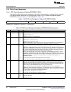
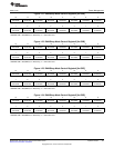
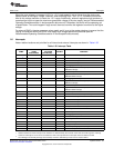
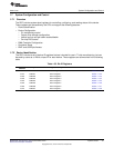
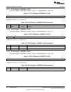
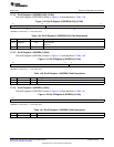
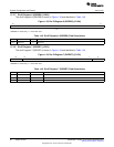
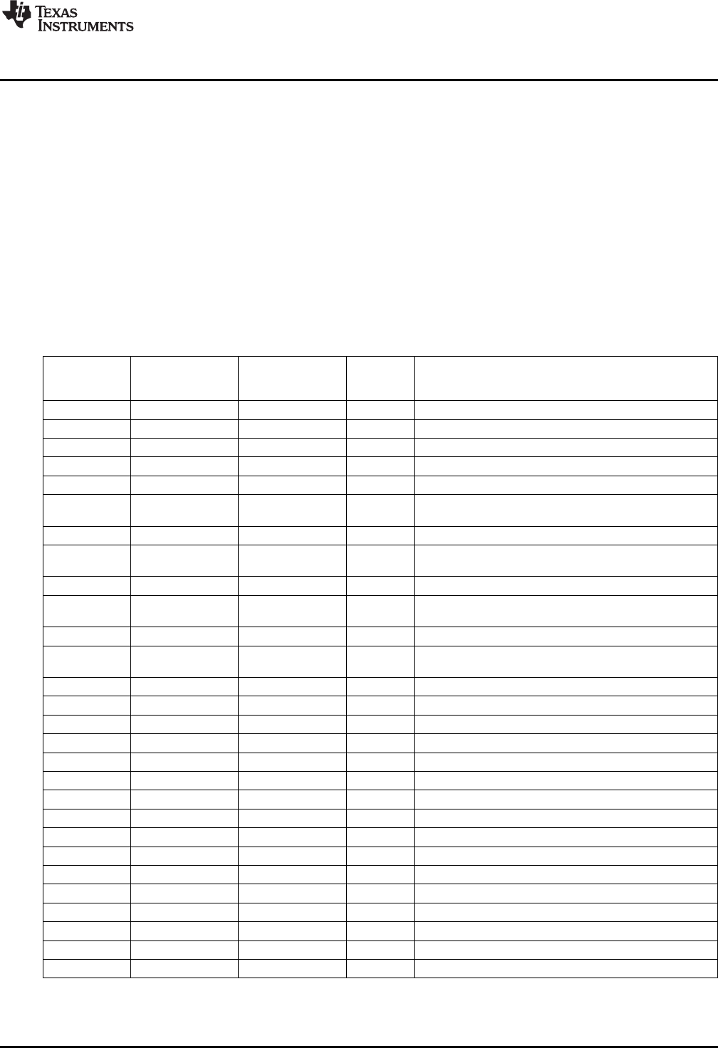
Vector-relative locations and priorities for all internal and external interrupts are shown in Table 1-32.
Table 1-32. Interrupt Table
SOFTWARE RELATIVE
NAME (TRAP) LOCATION PRIORITY FUNCTION
EQUIVALENT (HEX BYTES)
(1)
RESET SINT0 0x0 0 Reset (hardware and software)
NMI
(2)
SINT1 0x8 1 Non-maskable interrupt
INT0 SINT2 0x10 3 External user interrupt #0
INT1 SINT3 0x18 5 External user interrupt #1
TINT SINT4 0x20 6 Timer aggregated interrupt
PROG0 SINT5 0x28 7 Programmable transmit interrupt 0 (I2S0 transmit or
MMC/SD0 interrupt)
UART SINT6 0x30 9 UART interrupt
PROG1 SINT7 0x38 10 Programmable receive interrupt 1 (I2S0 receive or
MMC/SD0 SDIO interrupt)
DMA SINT8 0x40 11 DMA aggregated interrupt
PROG2 SINT9 0x48 13 Programmable transmit interrupt 1 (I2S1 transmit or
MMC/SD1 interrupt)
- SINT10 0x50 14 Software interrupt
PROG3 SINT11 0x58 15 Programmable receive interrupt 3 (I2S1 Receive or
MMC/SD1 SDIO interrupt)
LCD SINT12 0x60 17 LCD interrupt
SAR SINT13 0x68 18 10-bit SAR A/D conversion or pin interrupt
XMT2 SINT14 0x70 21 I2S2 transmit interrupt
RCV2 SINT15 0x78 22 I2S2 receive interrupt
XMT3 SINT16 0x80 4 I2S3 transmit interrupt
RCV3 SINT17 0x88 8 I2S3 receive interrupt
RTC SINT18 0x90 12 Wakeup or real-time clock interrupt
SPI SINT19 0x98 16 SPI interrupt
USB SINT20 0xA0 19 USB Interrupt
GPIO SINT21 0xA8 20 GPIO aggregated interrupt
EMIF SINT22 0xB0 23 EMIF error interrupt
I2C SINT23 0xB8 24 I2C interrupt
BERR SINT24 0xC0 2 Bus error interrupt
DLOG SINT25 0xC8 25 Data log interrupt
RTOS SINT26 0xD0 26 Real-time operating system interrupt
- SINT27 0xD8 14 Software interrupt #27
(1)
Absolute addresses of the interrupt vector locations are determined by the contents of the IVPD and IVPH registers. Interrupt
vectors for interrupts 0-15 and 24-31 are relative to IVPD. Interrupt vectors for interrupts 16-23 are relative to IVPH.
(2)
The NMI signal is internally tied high (not asserted). However, NMI interrupt vector can be used for SINT1.
53
SPRUFX5A–October 2010–Revised November 2010 System Control
Submit Documentation Feedback
Copyright © 2010, Texas Instruments Incorporated