


Theory of Operation
1705A Spectrum Monitor
4-3
bright-up signal, centered around the center frequency, is generated for the
Z--Axis Control circuit by the Marker Generator.
The Z--Axis Control circuit provides the driving signal for the Z--Axis Amplifier
(Diagram 8). Included in these unblanking signals are the sweep unblanking,
readout unblanking, and the intensified marker. This circuit controls both
display and readout intensity and adding the intensified marker in FULL
SPAN/DIV.
The output signal from the Log Detector (Diagram 2) is buffered and switched in
and out, for time sharing with the readout signal, prior to driving the Vertical
Output Amplifier. The output amplifier normalizes gain and matches the crt
deflection plate input impedance.
The ramp signal from the Sweep Generator (Diagram 3) is buffered, inverted,
and has its gain set prior to being used to drive the Horizontal Output Amplifier.
Like the Vertical Output Amplifier, the readout signal is time shared with active
signal. The horizontal amplifier has approximately three times the gain of the
vertical amplifier to meet the crt gain requirements.
The microprocessor, along with the EPROM that contains the measurement and
diagnostic routines, is the controlling element of the 1705A. A Non-Volatile
Random Access Memory (NVRAM) provides a method to store the current
front-panel switch settings, at power down, so that the 1705A can come back up
with the last front-panel setup.
CENTER FREQUENCY readout data is converted to digital data by an
Analog-to-Digital Converter and then input into the microprocessor. Readout
data and the Readout Enable (/RO--EN) are output from the microprocessor. The
readout data is converted back to an analog signal by the Digital-to-Analog
Converter.
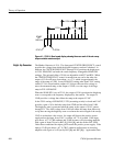
All of the switching and external control for the 1705A is shown on this
diagram. Control voltages are limited to 11.8 V or less. All switching is done in
conjunction with the microprocessor (Diagram 5). Indicator lights, that are
controlled by the microprocessor, are also included on this diagram.
The +18 V supply that is designed to drive an external Block Down Converter is
also shown on this schematic. The On/Off switch for the +18 V supply is
located on the 1705A rear panel.
The Low Voltage Power Supply converts the mains ac line voltage to 4 dc output
voltages (--15 V, +5 V, +15 V, and +40 V). The +40 V is used to power the
Vertical Deflection Amplifier (Diagram 4). The + and --15 V supplies are post
Deflection Amplifiers
(Diagram 4)
Microprocessor
(Diagram 5)
Front Panel (Diagram 6)
Low Voltage Power Supply
(Diagram 7)