


Serial Host Interface Internal Architecture
DSP56366 24-Bit Digital Signal Processor User Manual, Rev. 4
7-2 Freescale Semiconductor
7.2 Serial Host Interface Internal Architecture
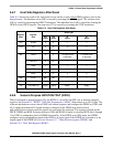
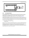
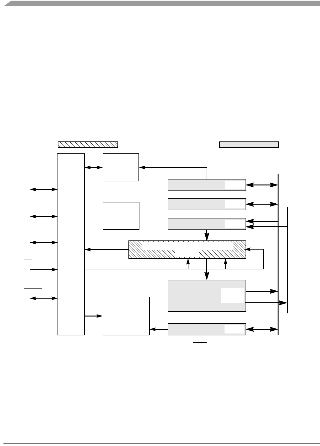
The DSP views the SHI as a memory-mapped peripheral in the X data memory space. The DSP uses the
SHI as a normal memory-mapped peripheral using standard polling or interrupt programming techniques
and DMA transfers. Memory mapping allows DSP communication with the SHI registers to be
accomplished using standard instructions and addressing modes. In addition, the MOVEP instruction
allows interface-to-memory and memory-to-interface data transfers without going through an intermediate
register. The DMA controller may be used to service the receive or transmit data path. The single master
configuration allows the DSP to directly connect to dumb peripheral devices. For that purpose, a
programmable baud-rate generator is included to generate the clock signal for serial transfers. The host
side invokes the SHI for communication and data transfer with the DSP through a shift register that may
be accessed serially using either the I
2
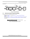
C or the SPI bus protocols. Figure 7-1 shows the SHI block diagram.
Figure 7-1 Serial Host Interface Block Diagram
7.3 SHI Clock Generator
The SHI clock generator generates the SHI serial clock if the interface operates in the master mode. The
clock generator is disabled if the interface operates in the slave mode, except in I
2
C mode when the
HCKFR bit is set in the HCKR register. When the SHI operates in the slave mode, the clock is external
and is input to the SHI (HMST = 0). Figure 7-2 illustrates the internal clock path connections. It is the
DSP
Global
Data
Bus
DSP AccessibleHost Accessible
SCK/SCL
MISO/SDA
MOSI/HA0
SS
/HA2
HRX
(FIFO)
HREQ
HCSR
HTX
HCKR
24 BIT
HSAR
Clock
Generator
Controller
Logic
Slave
Address
Recognition
Unit
(SAR)
Pin
Control
Logic
INPUT/OUTPUT Shift Register
(IOSR)
AA0416
DSP
DMA
Data
Bus