


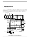
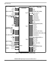

DSP56300 Core Functional Blocks
DSP56366 24-Bit Digital Signal Processor User Manual, Rev. 4
1-6 Freescale Semiconductor
• Nested hardware DO loops
• Fast auto-return interrupts
The PCU implements its functions using the following registers:
• PC—program counter register
• SR—Status register
• LA—loop address register
• LC—loop counter register
• VBA—vector base address register
• SZ—stack size register
• SP—stack pointer
• OMR—operating mode register
• SC—stack counter register
The PCU also includes a hardware system stack (SS).
1.4.4 Internal Buses
To provide data exchange between blocks, the following buses are implemented:
• Peripheral input/output expansion bus (PIO_EB) to peripherals
• Program memory expansion bus (PM_EB) to program memory
• X memory expansion bus (XM_EB) to X memory
• Y memory expansion bus (YM_EB) to Y memory
• Global data bus (GDB) between registers in the DMA, AGU, OnCE, PLL, BIU, and PCU as well
as the memory-mapped registers in the peripherals
• DMA data bus (DDB) for carrying DMA data between memories and/or peripherals
• DMA address bus (DAB) for carrying DMA addresses to memories and peripherals
• Program Data Bus (PDB) for carrying program data throughout the core
• X memory Data Bus (XDB) for carrying X data throughout the core
• Y memory Data Bus (YDB) for carrying Y data throughout the core
• Program address bus (PAB) for carrying program memory addresses throughout the core
• X memory address bus (XAB) for carrying X memory addresses throughout the core
• Y memory address bus (YAB) for carrying Y memory addresses throughout the core
All internal buses on the DSP56300 family members are 24-bit buses. See Figure 1-1.
1.4.5 Direct Memory Access (DMA)
The DMA block has the following features:
• Six DMA channels supporting internal and external accesses
• One-, two-, and three-dimensional transfers (including circular buffering)