


DSP56300 Core Description
DSP56366 24-Bit Digital Signal Processor User Manual, Rev. 4
1-2 Freescale Semiconductor
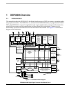
1.2 DSP56300 Core Description
The DSP56366 uses the DSP56300 core, a high-performance, single clock cycle per instruction engine that
provides up to twice the performance of Freescale's popular DSP56000 core family while retaining code
compatibility with it.
The DSP56300 core family offers a new level of performance in speed and power, provided by its rich
instruction set and low power dissipation, thus enabling a new generation of wireless, telecommunications,
and multimedia products. For a description of the DSP56300 core, see Section 1.4, "DSP56300 Core
Functional Blocks". Significant architectural enhancements to the DSP56300 core family include a barrel
shifter, 24-bit addressing, an instruction cache, and direct memory access (DMA).
The DSP56300 core family members contain the DSP56300 core and additional modules. The modules
are chosen from a library of standard predesigned elements such as memories and peripherals. New
modules may be added to the library to meet customer specifications. A standard interface between the
DSP56300 core and the on-chip memory and peripherals supports a wide variety of memory and
peripheral configurations. Refer to Section 3, "Memory Configuration".
Core features are described fully in the DSP56300 Family Manual. Pinout, memory, and peripheral
features are described in this manual.
• DSP56300 modular chassis
— 120 Million Instructions Per Second (MIPS) with an 120 MHz clock at 3.3V.
— Object Code Compatible with the 56K core.
— Data ALU with a 24 × 24 bit multiplier-accumulator and a 56-bit barrel shifter. 16-bit
arithmetic support.
— Program Control with position independent code support and instruction cache support.
— Six-channel DMA controller.
— PLL based clocking with a wide range of frequency multiplications (1 to 4096), predivider
factors (1 to 16) and power saving clock divider (2
i
: i=0 to 7). Reduces clock noise.
— Internal address tracing support and OnCE™ for Hardware/Software debugging.
— JTAG port.
— Very low-power CMOS design, fully static design with operating frequencies down to DC.
— STOP and WAIT low-power standby modes.
• On-chip Memory Configuration
—7K × 24 Bit Y-Data RAM and 8K × 24 Bit Y-Data ROM.
— 13K × 24 Bit X-Data RAM and 32K × 24 Bit X-Data ROM.
— 40K × 24 Bit Program ROM.
—3K × 24 Bit Program RAM and 192 × 24 Bit Bootstrap ROM. 1K of Program RAM may be
used as Instruction Cache or for Program ROM patching.
—2K × 24 Bit from Y Data RAM and 5K × 24 Bit from X Data RAM can be switched to Program
RAM resulting in up to 10K × 24 Bit of Program RAM.
• Off-chip memory expansion
— External Memory Expansion Port.