


DAX Programming Considerations
DSP56366 24-Bit Digital Signal Processor User Manual, Rev. 4
10-10 Freescale Semiconductor
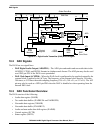
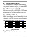
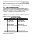
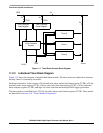
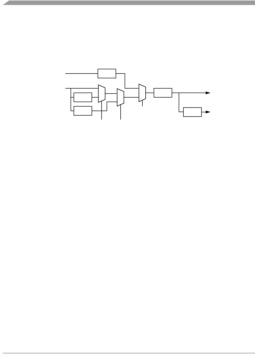
• The internal DSP core clock—assumes 1024 × Fs
• DAX clock input pin (ACI)—512 × Fs
• DAX clock input pin (ACI)—384 × Fs
• DAX clock input pin (ACI)—256 × Fs
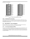
Figure 10-5 shows how each clock is divided to generate the biphase and bit shift clocks
Figure 10-5 Clock Multiplexer Diagram
NOTE
For proper operation of the DAX, the DSP core clock frequency must be at
least five times higher than the DAX bit shift clock frequency (64 × Fs).
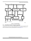
10.5.12 DAX State Machine
The DAX state machine generates a set of sequencing signals used in the DAX.
10.6 DAX Programming Considerations
The following sections describe programming considerations for the DAX.
10.6.1 Initiating A Transmit Session
To initiate the DAX operation, follow this procedure:
1. Ensure that the DAX is disabled (PC1 and PC0 bits of port control register PCR are cleared)
2. Write the non-audio data to the corresponding bits in the XNADR register
3. Write the channel A and channel B audio data in the XADR register
4. Write the transmit mode to the XCTR register
5. Enable DAX by setting PC1 bit (and by setting PC0 bit if in slave mode) in the port control register
(PCR); transmission begins.
10.6.2 Audio Data Register Empty Interrupt Handling
When the XDIE bit is set and the DAX is active, an audio data register empty interrupt (XADE = 1) is
generated once at the beginning of every frame transmission. Typically, within an XADE interrupt, the
1/4
2/3
1/2
1/2
1/2
Biphase
Clock
(128
× Fs)
Bit Shift
Clock
(64
× Fs)
DSP Core Clock
(1024
× Fs)
ACI Pin
{256,384,512}
× Fs
(XCS1 or XCS0)
XCS0
1
0
XCS1
1
0
1
0
MUX
MUX
MUX
AA0610