


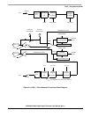

ESAI_1 Programming Model
DSP56366 24-Bit Digital Signal Processor User Manual, Rev. 4
Freescale Semiconductor 9-11
9.3.8 ESAI_1 Receive Shift Registers
The receive shift registers receive the incoming data from the serial receive data pins. Data is shifted in by
the selected (internal/external) bit clock when the associated frame sync I/O is asserted. Data is assumed
to be received MSB first if RSHFD=0 and LSB first if RSHFD=1. Data is transferred to the ESAI_1
receive data registers after 8, 12, 16, 20, 24, or 32 serial clock cycles were counted, depending on the slot
length control bits in the RCR_1 register.
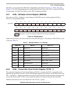
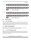
9.3.9 ESAI_1 Receive Data Registers
The Receive Data Registers RX3_1, RX2_1, RX1_1, and RX0_1 are 24-bit read-only registers that accept
data from the receive shift registers when they become full. The data occupies the most significant portion
of the receive data registers, according to the ALC control bit setting. The unused bits (least significant
portion, and 8 most significant bits when ALC=1) read as zeros. The DSP is interrupted whenever RXx_1
becomes full if the associated interrupt is enabled.
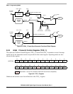
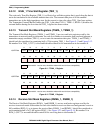
9.3.10 ESAI_1 Transmit Shift Registers
The Transmit Shift Registers contain the data being transmitted. Data is shifted out to the serial transmit
data pins by the selected (internal/external) bit clock when the associated frame sync I/O is asserted. The
number of bits shifted out before the shift registers are considered empty and may be written to again can
be 8, 12, 16, 20, 24 or 32 bits (determined by the slot length control bits in the TCR_1 register). Data is
shifted out of these registers MSB first if TSHFD=0 and LSB first if TSHFD=1.
9.3.11 ESAI_1 Transmit Data Registers
The Transmit Data registers TX5_1, TX4_1, TX3_1, TX2_1, TX1_1, and TX0_1 are 24-bit write-only
registers. Data to be transmitted is written into these registers and is automatically transferred to the
transmit shift registers. The data written (8, 12, 16, 20 or 24 bits) should occupy the most significant
portion of the TXx_1 according to the ALC control bit setting. The unused bits (least significant portion,
and the 8 most significant bits when ALC=1) of the TXx_1 are don’t care bits. The DSP is interrupted
whenever the TXx_1 becomes empty if the transmit data register empty interrupt has been enabled.
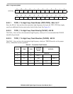
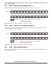
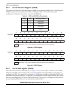
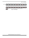
11109876543210
Y:$FFFF93 RODF REDF RDF ROE RFS IF2 IF1 IF0
23 22 21 20 19 18 17 16 15 14 13 12
TODE TEDE TDE TUE TFS
Reserved bit - read as zero; should be written with zero for future compatibility.
Figure 9-10 SAISR_1 Register