


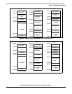
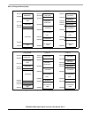
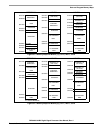
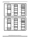
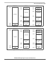
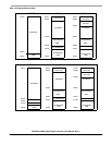
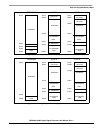
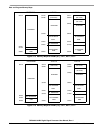
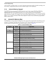

Data and Program Memory Maps
DSP56366 24-Bit Digital Signal Processor User Manual, Rev. 4
Freescale Semiconductor 3-11
3.1.1 Reserved Memory Spaces
The reserved memory spaces should not be accessed by the user. They are reserved for future expansion.
3.1.2 Program ROM Area Reserved for Freescale Use
The last 128 words ($FFAF80-$FFAFFF) of the Program ROM are reserved for Freescale use. This
memory area is reserved for use as expansion area for the bootstrap ROM as well as for testing purposes.
Customer code should not use this area. The contents of this Program ROM segment is defined by the
Appendix A, "Bootstrap ROM Contents".
3.1.3 Bootstrap ROM
The 192-word Bootstrap ROM occupies locations $FF0000-$FF00BF. The bootstrap ROM is
factory-programmed to perform the bootstrap operation following hardware reset. The contents of the
Bootstrap ROM are defined by the Bootstrap ROM source code in Appendix A, "Bootstrap ROM
Contents".
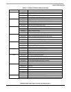
3.1.4 Dynamic Memory Configuration Switching
The internal memory configuration is altered by re-mapping RAM modules from Y and X data memory
into program memory space and vice-versa. The contents of the switched RAM modules are preserved.
The memory can be dynamically switched from one configuration to another by changing the MS, MSW0
or MSW1 bits in OMR. The address ranges that are directly affected by the switch operation are specified
in Table 3-2. The memory switch can be accomplished provided that the affected address ranges are not
being accessed during the instruction cycle in which the switch operation takes place. Accordingly, the
following condition must be observed for trouble-free dynamic switching:
NOTE
No accesses (including instruction fetches) to or from the affected address
ranges in program and data memories are allowed during the switch cycle.
NOTE
The switch cycle actually occurs 3 instruction cycles after the instruction
that modifies the MS, MSW0 or MSW1 bits.
Any sequence that complies with the switch condition is valid. For example, if the program flow executes
in the address range that is not affected by the switch, the switch condition can be met very easily. In this
case a switch can be accomplished by just changing the MS, MSW0 or MSW1 bits in OMR in the regular
program flow, assuming no accesses to the affected address ranges of the data memory occur up to 3
instructions after the instruction that changes the OMR bit. Special care should be taken in relation to the
interrupt vector routines since an interrupt could cause the DSP to fetch instructions out of sequence and
might violate the switch condition.
Special attention should be given when running a memory switch routine using the OnCE™ port. Running
the switch routine in Trace mode, for example, can cause the switch to complete after the MS bit change