


Programming Sheets
DSP56366 24-Bit Digital Signal Processor User Manual, Rev. 4
Freescale Semiconductor D-27
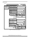
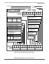
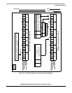
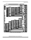
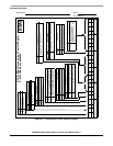
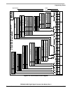
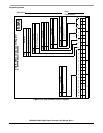
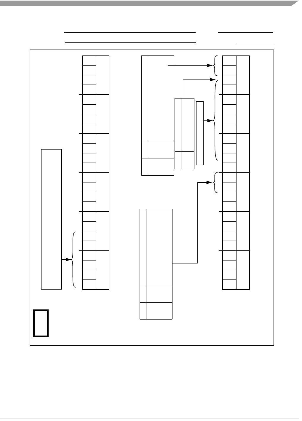
Figure D-12. SHI Slave Address and Clock Control Registers
10
Application:
Date:
Programmer:
Sheet 1 of 3
SHI
15 14 13 12
11 9876543210
HDM4 HDM2HDM1HDM0 HRS CPOLCPHA
SHI Clock Control
X:$FFFF90
Reset = $000001
Register (HCKR)
19 18 17 1623 22 21 20
*
0
*
0
HDM3
*
0
HDM7
*
0
*
0
*
0
*
0
15 14 13 12
11109876543210
SHI Slave Address
X:$FFFF92
Reset = $Bx0000
Register (HSAR)
19 18 17 1623 22 21 20
HA1HA3HA5
*
0
*
0
HA6
*
0
*
0
*
0
*
0
*
0
*
0
*
0
*
0
*
0
*
0
*
0
*
0
*
0
*
0
*
0
*
0
*
0
HA4
0000
*
0
*
0
*
0
*
0
00
HDM5
HCKR Divider Modulus
HSAR I
2
C Slave Address
Slave address = Bits HA6-HA3, HA1 and external pins HA2, HA0
Slave address after reset = 1011[HA2]0[HA0]
HFM1 HFM0 SHI Noise Reduction Filter Mode
0 0 Bypassed (Filter disabled)
01 Reserved
1 0 Narrow spike tolerance
1 1 Wide spike tolerance
HFM0HFM1
SHI Clock Control Register (HCKR)
SHI Slave Address Register (HSAR)
CPOL CPHA Result
0 0 SCK active low, strobe on rising edge
0 1 SCK active low, strobe on falling edge
1 0 SCK active high, strobe on falling edge
1 1 SCK active high, strobe on rising edge
HRS Result
0 Prescaler operational
1 Prescaler bypassed
HDM6
*
= Reserved, write as 0