


SHI Programming Considerations
DSP56366 24-Bit Digital Signal Processor User Manual, Rev. 4
Freescale Semiconductor 7-19
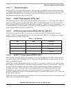
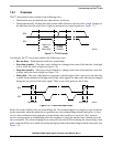
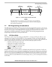
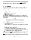
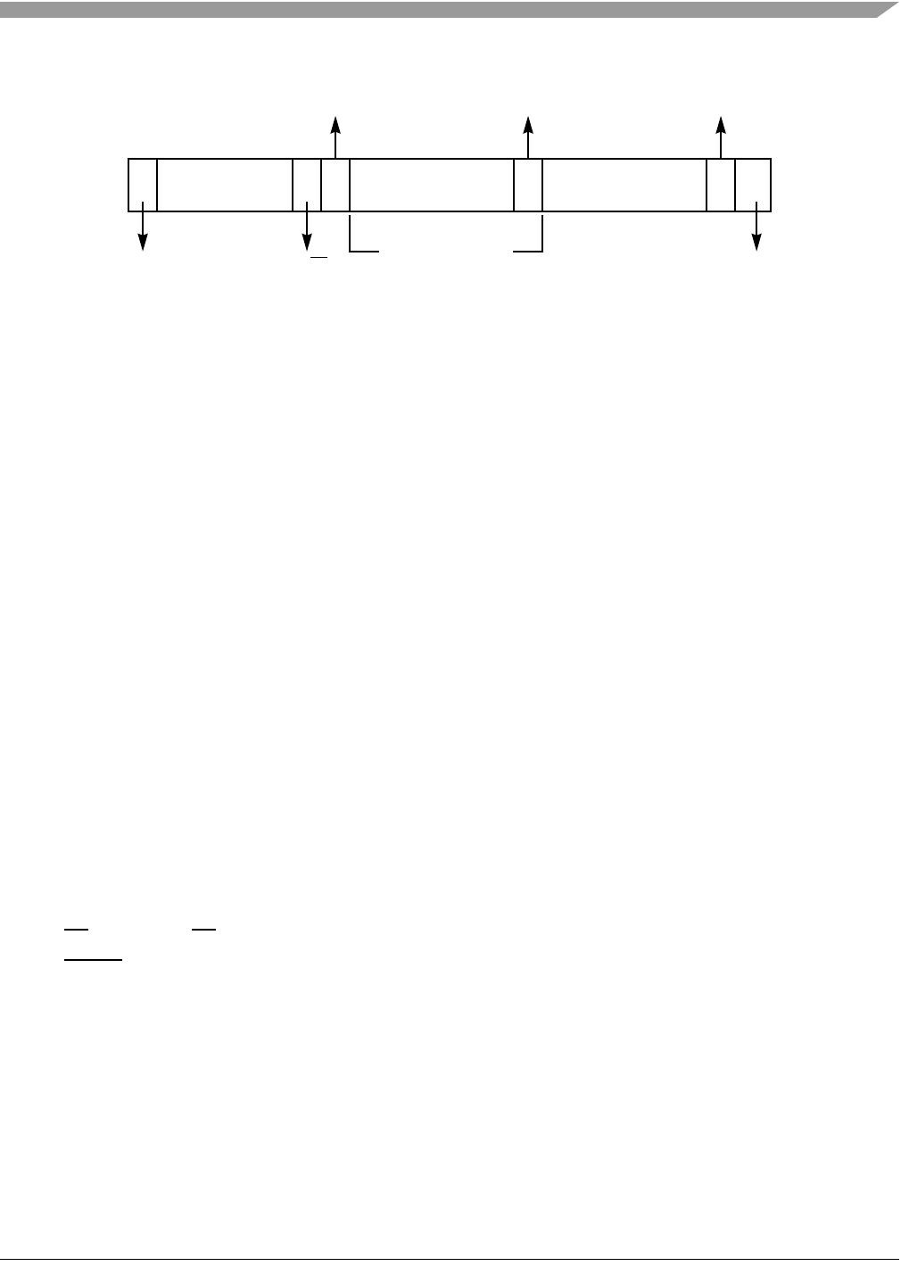
Figure 7-11 I
2
C Bus Protocol For Host Read Cycle
NOTE
The first data byte in a write-bus cycle can be used as a user-predefined
control byte (e.g., to determine the location to which the forthcoming data
bytes should be transferred).
7.7 SHI Programming Considerations
The SHI implements both SPI and I
2
C bus protocols and can be programmed to operate as a slave device
or a single-master device. Once the operating mode is selected, the SHI may communicate with an external
device by receiving and/or transmitting data. Before changing the SHI operational mode, an SHI
individual reset should be generated by clearing the HEN bit. The following paragraphs describe
programming considerations for each operational mode.
7.7.1 SPI Slave Mode
The SPI slave mode is entered by enabling the SHI (HEN=1), selecting the SPI mode (HI
2
C=0), and
selecting the slave mode of operation (HMST=0). The programmer should verify that the CPHA and
CPOL bits (in the HCKR) correspond to the external host clock phase and polarity. Other HCKR bits are
ignored. When configured in the SPI slave mode, the SHI external pins operate as follows:
• SCK/SCL is the SCK serial clock input.
• MISO/SDA is the MISO serial data output.
• MOSI/HA0 is the MOSI serial data input.
•SS
/HA2 is the SS slave select input.
•HREQ
is the Host Request output.
In the SPI slave mode, a receive, transmit, or full-duplex data transfer may be performed. Actually, the
interface performs data receive and transmit simultaneously. The status bits of both receive and transmit
paths are active; however, the programmer may disable undesired interrupts and ignore irrelevant status
bits. It is recommended that an SHI individual reset (HEN cleared) be generated before beginning data
reception in order to reset the HRX FIFO to its initial (empty) state (e.g., when switching from transmit to
receive data).
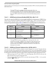
SAA1Slave Address
R/W
P 1
Start Stop
Bit Bit
Slave Device
ACK from
Master Device
ACK from
No ACK
Data Byte
N = 0 to M
Data Bytes
Last Data Byte
from Master Device
AA0426