


Programming Sheets
DSP56366 24-Bit Digital Signal Processor User Manual, Rev. 4
D-32 Freescale Semiconductor
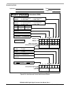
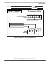
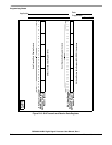
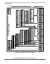
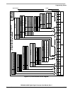
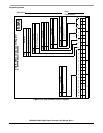
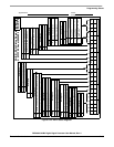
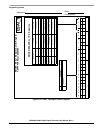
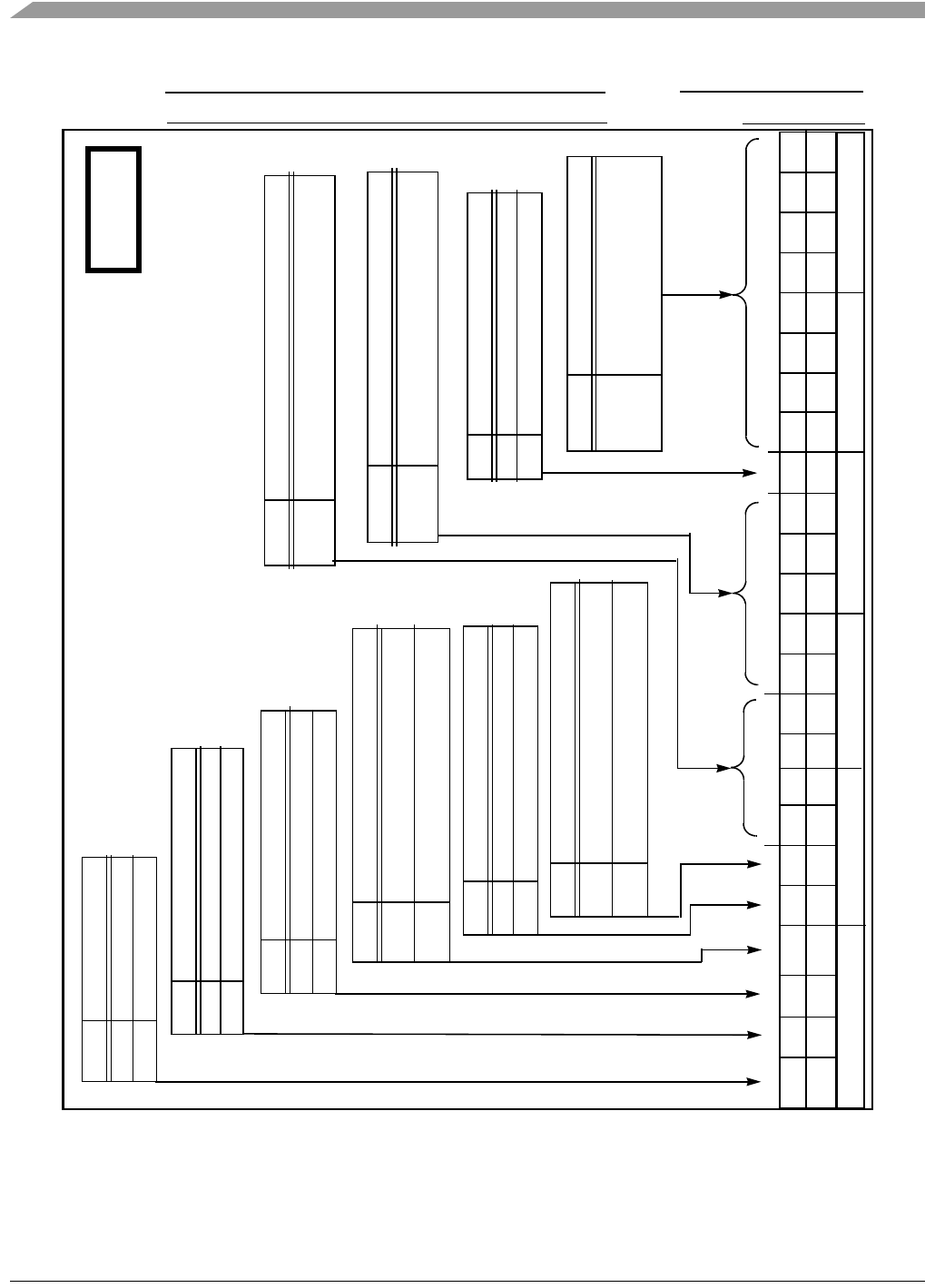
Figure D-17. ESAI Receive Clock Control Register
15 6 5 419 18 17 16 10 9 8 714 13 12 11
RPM0
3210
RPM2
23 22 21 20
RPM1
RPM3RPM4RPM5RPM6RPM7RPSRRDC0RDC1RDC2RDC3RDC4RFP0RFP1RFP2RFP3RCKPRFSPRHCKPRCKDRFSDRHCKD
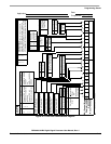
RCKP
Description
0
1
Clockout on rising edge of receive clock,
latch in on falling edge of receive clock
Clockout on falling edge of receive clock,
latch in on rising edge of receive clock
RFSP Description
0
1
Frame sync polarity positive
Frame sync polarity negative
RFP [3:0] Description
Sets divide rate for receiver high frequency clock
RCKD
Description
0
1
External clock source used
Internal clock source
RFSD
Description
0
1
FSR is input
FSR is output
RHCKD
Description
0
1
HCKR is input
HCKR is output
RHCKP Description
0
1
Clockout on rising edge of receive clock,
latch in on falling edge of receive clock
Clockout on falling edge of receive clock,
latch in on rising edge of receive clock
Range $0 - $F (1 -16). See 8.3.3.4
RDC [4:0] Description
Controls frame rate dividers
RPM [7:0] Description
Specifies prescaler ratio for the
RPSR Description
0
1
Divide by 8 prescaler operational
Divide by 8 prescaler bypassed
Range from $00 - $FF (1 - 256).
receive clock generator
See 8.3.3.1
ESAI
RCCR - ESAI Receive Clock Control Register
X: $FFFFB8 Reset: $000000
Range 00000 - 11111 (1-32) See 8.3.3.2
Application:
Date:
Programmer: