


Enhanced Serial Audio Interface
DSP56366 24-Bit Digital Signal Processor User Manual, Rev. 4
Freescale Semiconductor 2-15
2.9 Enhanced Serial Audio Interface
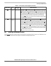
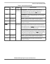
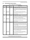
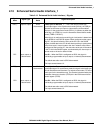
Table 2-11 Enhanced Serial Audio Interface Signals
Signal Name Signal Type
State during
Reset
Signal Description
HCKR Input or output GPIO
disconnected
High Frequency Clock for Receiver — When programmed as an
input, this signal provides a high frequency clock source for the ESAI
receiver as an alternate to the DSP core clock. When programmed as
an output, this signal can serve as a high-frequency sample clock (e.g.,
for external digital to analog converters [DACs]) or as an additional
system clock.
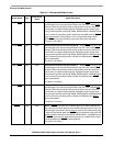
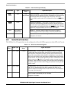
PC2 Input, output, or
disconnected
Port C 2 — When the ESAI is configured as GPIO, this signal is
individually programmable as input, output, or internally disconnected.
The default state after reset is GPIO disconnected.
This input is 5 V tolerant.
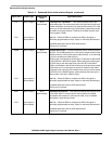
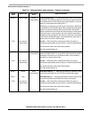
HCKT Input or output GPIO
disconnected
High Frequency Clock for Transmitter — When programmed as an
input, this signal provides a high frequency clock source for the ESAI
transmitter as an alternate to the DSP core clock. When programmed as
an output, this signal can serve as a high frequency sample clock (e.g.,
for external DACs) or as an additional system clock.
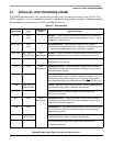
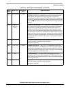
PC5 Input, output, or
disconnected
Port C 5 — When the ESAI is configured as GPIO, this signal is
individually programmable as input, output, or internally disconnected.
The default state after reset is GPIO disconnected.
This input is 5 V tolerant.
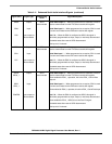
FSR Input or output GPIO
disconnected
Frame Sync for Receiver — This is the receiver frame sync
input/output signal. In the asynchronous mode (SYN=0), the FSR pin
operates as the frame sync input or output used by all the enabled
receivers. In the synchronous mode (SYN=1), it operates as either the
serial flag 1 pin (TEBE=0), or as the transmitter external buffer enable
control (TEBE=1, RFSD=1).
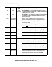
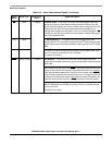
When this pin is configured as serial flag pin, its direction is determined
by the RFSD bit in the RCCR register. When configured as the output
flag OF1, this pin will reflect the value of the OF1 bit in the SAICR
register, and the data in the OF1 bit will show up at the pin synchronized
to the frame sync in normal mode or the slot in network mode. When
configured as the input flag IF1, the data value at the pin will be stored
in the IF1 bit in the SAISR register, synchronized by the frame sync in
normal mode or the slot in network mode.
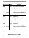
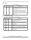
PC1 Input, output, or
disconnected
Port C 1 — When the ESAI is configured as GPIO, this signal is
individually programmable as input, output, or internally disconnected.
The default state after reset is GPIO disconnected.
This input is 5 V tolerant.