


ESAI Programming Model
DSP56366 24-Bit Digital Signal Processor User Manual, Rev. 4
Freescale Semiconductor 8-25
In the synchronous mode when RCKD is set, the SCKR pin becomes the OF0 output flag. If RCKD is
cleared, then the SCKR pin becomes the IF0 input flag. See Table 8-1 and Table 8-7
.
8.3.3.9 RCCR Receiver Frame Sync Signal Direction (RFSD) - Bit 22
The Receiver Frame Sync Signal Direction (RFSD) bit selects the source of the receiver frame sync signal
when in the asynchronous mode (SYN=0), and the IF1/OF1/Transmitter Buffer Enable flag direction in
the synchronous mode (SYN=1).
In the asynchronous mode when RFSD is set, the internal clock generator becomes the source of the
receiver frame sync, and is the output on the FSR pin. In the asynchronous mode when RFSD is cleared,
the receiver frame sync source is external; the internal clock generator is disconnected from the FSR pin,
and an external clock source may drive this pin.
In the synchronous mode when RFSD is set, the FSR pin becomes the OF1 output flag or the Transmitter
Buffer Enable, according to the TEBE control bit. If RFSD is cleared, then the FSR pin becomes the IF1
input flag. See Table 8-1 and Table 8-8.
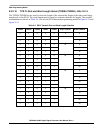
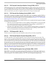
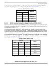
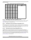
Table 8-7 SCKR Pin Definition Table
Control Bits
SCKR PIN
SYN RCKD
0 0 SCKR input
0 1 SCKR output
10 IF0
11OF0
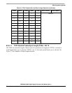
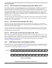
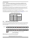
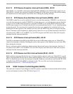
Table 8-8 FSR Pin Definition Table
Control Bits
FSR Pin
SYN TEBE RFSD
0 X 0 FSR input
0 X 1 FSR output
100 IF1
101 OF1
110 reserved
1 1 1 Transmitter Buffer Enable